SLUSAQ3H November 2011 – June 2024 UCC27523 , UCC27525 , UCC27526
PRODUCTION DATA
- 1
- 1 Features
- 2 Applications
- 3 Description
- 4 Description (continued)
- 5 Pin Configuration and Functions
- 6 Specifications
- 7 Detailed Description
- 8 Application and Implementation
- 9 Power Supply Recommendations
- 10Layout
- 11Device and Documentation Support
- 12Revision History
- 13Mechanical, Packaging, and Orderable Information
6.6 Switching Characteristics
over operating free-air temperature range (unless otherwise noted)
| PARAMETER | TEST CONDITIONS | MIN | TYP | MAX | UNIT | |
|---|---|---|---|---|---|---|
| tR | Rise time (1) | CLOAD = 1.8 nF | 7 | 18 | ns | |
| tF | Fall time(1) | CLOAD = 1.8 nF | 6 | 10 | ||
| tM | Delay matching between 2 channels | INA = INB, OUTA and OUTB at 50% transition point | 1 | 4 | ||
| tPW | Minimum input pulse width that changes the output state | 15 | 25 | |||
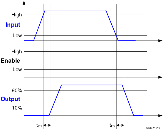
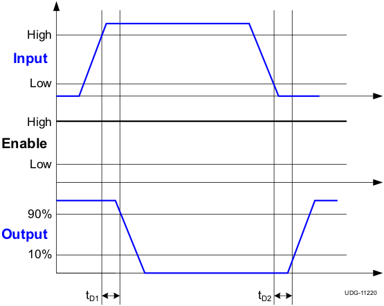
| tD1, tD2 | Input to output propagation delay (1) | CLOAD = 1.8 nF, 5-V input pulse | 6 | 13 | 23 | |
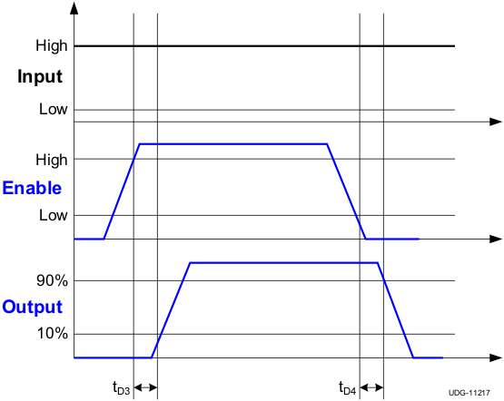
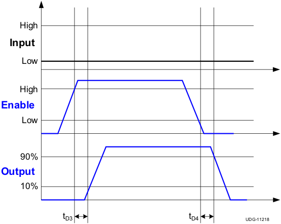
| tD3, tD4 | EN to output propagation delay (1) | CLOAD = 1.8 nF, 5-V enable pulse | 6 | 13 | 23 | |
 Figure 6-1 Enable Function (For Non-Inverting Input Driver Operation)
 Figure 6-3 Non-Inverting Input Driver Operation
 Figure 6-2 Enable Function (For Inverting Input Driver Operation)
 Figure 6-4 Inverting Input Driver Operation