SLUSB80E September   2012  – January 2018 BQ24157

PRODUCTION DATA.  

  1. Features
  2. Applications
  3. Description
  4. Revision History
  5. Description (Continued)
  6. Device Comparisons
  7. Pin Configuration and Functions
  8. Specifications
    1. 8.1 Absolute Maximum Ratings
    2. 8.2 ESD Ratings
    3. 8.3 Recommended Operating Conditions
    4. 8.4 Thermal Information
    5. 8.5 Electrical Characteristics
    6. 8.6 Timing Requirements
    7. 8.7 Typical Characteristics
  9. Detailed Description
    1. 9.1 Overview
    2. 9.2 Functional Block Diagrams
    3. 9.3 Operational Flow Chart
    4. 9.4 Feature Description
      1. 9.4.1 Input Voltage Protection
        1. 9.4.1.1 Input Overvoltage Protection
        2. 9.4.1.2 Bad Adaptor Detection/Rejection
        3. 9.4.1.3 Sleep Mode
        4. 9.4.1.4 Input Voltage Based DPM (Special Charger Voltage Threshold)
      2. 9.4.2 Battery Protection
        1. 9.4.2.1 Output Overvoltage Protection
        2. 9.4.2.2 Battery Detection at Power Up in DEFAULT Mode
        3. 9.4.2.3 Battery Short Protection
        4. 9.4.2.4 Battery Detection in Host Mode
      3. 9.4.3 DEFAULT Mode
      4. 9.4.4 USB Friendly Power Up
      5. 9.4.5 Input Current Limiting At Power Up
    5. 9.5 Device Functional Modes
      1. 9.5.1 Charge Mode Operation
        1. 9.5.1.1 Charge Profile
      2. 9.5.2 PWM Controller in Charge Mode
      3. 9.5.3 Battery Charging Process
      4. 9.5.4 Thermal Regulation and Protection
      5. 9.5.5 Charge Status Output, STAT Pin
      6. 9.5.6 Control Bits in Charge Mode
        1. 9.5.6.1 CE Bit (Charge Mode)
        2. 9.5.6.2 RESET Bit
        3. 9.5.6.3 OPA_Mode Bit
      7. 9.5.7 Control Pins in Charge Mode
        1. 9.5.7.1 CD Pin (Charge Disable)
      8. 9.5.8 BOOST Mode Operation
        1. 9.5.8.1 PWM Controller in Boost Mode
        2. 9.5.8.2 Boost Start Up
        3. 9.5.8.3 PFM Mode at Light Load
        4. 9.5.8.4 Protection in Boost Mode
          1. 9.5.8.4.1 Output Overvoltage Protection
          2. 9.5.8.4.2 Output Overload Protection
          3. 9.5.8.4.3 Battery Overvoltage Protection
        5. 9.5.8.5 STAT Pin in Boost Mode
      9. 9.5.9 High Impedance (Hi-Z) Mode
    6. 9.6 Programming
      1. 9.6.1 Serial Interface Description
        1. 9.6.1.1 F/S Mode Protocol
        2. 9.6.1.2 H/S Mode Protocol
        3. 9.6.1.3 I2C Update Sequence
        4. 9.6.1.4 Slave Address Byte
        5. 9.6.1.5 Register Address Byte
    7. 9.7 Register Description
  10. 10Application and Implementation
    1. 10.1 Application Information
      1. 10.1.1 Typical Application
        1. 10.1.1.1 Design Requirements
        2. 10.1.1.2 Detailed Design Procedure
      2. 10.1.2 Charge Current Sensing Resistor Selection Guidelines
      3. 10.1.3 Output Inductor and Capacitance Selection Guidelines
    2. 10.2 Typical Performance Curves
  11. 11Power Supply Recommendations
    1. 11.1 System Load After Sensing Resistor
      1. 11.1.1 The Advantages:
      2. 11.1.2 Design Requirements and Potential Issues:
  12. 12Layout
    1. 12.1 Layout Guidelines
    2. 12.2 Layout Example
  13. 13Device and Documentation Support
    1. 13.1 Documentation Support
      1. 13.1.1 Third-Party Products Disclaimer
    2. 13.2 Receiving Notification of Documentation Updates
    3. 13.3 Community Resources
    4. 13.4 Trademarks
    5. 13.5 Electrostatic Discharge Caution
    6. 13.6 Glossary
  14. 14Mechanical, Packaging, and Orderable Information
    1. 14.1 Package Summary
      1. 14.1.1 Chip Scale Packaging Dimensions

Pin Configuration and Functions

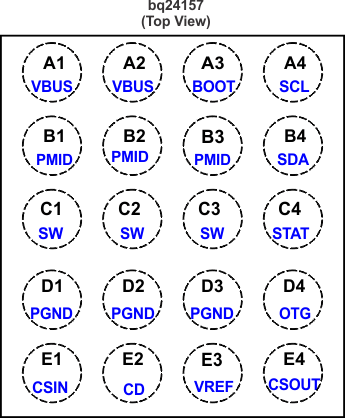
Pin Layout (20-Bump YFF Package)
bq24157 pinout_lusb80.gif

Pin Functions

PIN I/O DESCRIPTION
NAME NO.
BOOT A3 I/O Bootstrap capacitor connection for the high-side FET gate driver. Connect a 33-nF ceramic capacitor (voltage rating ≥ 10 V) from BOOT pin to SW pin.
CD E2 I Charge disable control pin. CD=0, charge is enabled. CD=1, charge is disabled and VBUS pin is high impedance to GND.
CSIN E1 I Charge current-sense input. Battery current is sensed across an external sense resistor. A 0.1-μF ceramic capacitor to PGND is required.
CSOUT E4 I Battery voltage and current sense input. Bypass it with a ceramic capacitor (minimum 0.1 μF) to PGND if there are long inductive leads to battery.
OTG D4 I Boost mode enable control or input current limiting selection pin. When OTG is in active status, the device is forced to operate in boost mode. It has higher priority over I2C control and can be disabled using the control register. At POR while in default mode, the OTG pin is used as the input current limiting selection pin. The I2C register is ignored at startup. When OTG=High, IIN_LIMIT = 500mA and when OTG = Low, IIN_LIMIT = 100mA.
PGND D1, D2, D3 Power ground
PMID B1, B2, B3 I/O Connection point between reverse blocking FET and high-side switching FET. Bypass it with a minimum of 3.3-μF capacitor from PMID to PGND.
SCL A4 I I2C interface clock. Connect a 10-kΩ pullup resistor to 1.8V rail (VAUX= VCC_HOST)
SDA B4 I/O I2C interface data. Connect a 10-kΩ pullup resistor to 1.8V rail (VAUX= VCC_HOST)
STAT C4 O Charge status pin. Pull low when charge in progress. Open drain for other conditions. During faults, a 128-μs pulse is sent out. STAT pin can be disabled by the EN_STAT bit in control register. STAT can be used to drive a LED or communicate with a host processor.
SW C1, C2, C3 O Internal switch to output inductor connection.
VBUS A1, A2 I/O Charger input voltage. Bypass it with a 1-μF ceramic capacitor from VBUS to PGND. It also provides power to the load during boost mode .
VREF E3 O Internal bias regulator voltage. Connect a 1µF ceramic capacitor from this output to PGND. External load on VREF is not recommended.