SLUSBD9A February 2013 – September 2024 UCC27532
PRODUCTION DATA
7.2 Typical Applications
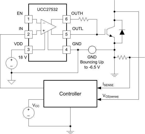 Figure 7-1 Driving IGBT Without Negative Bias
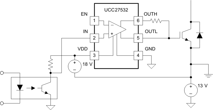 Figure 7-2 Driving IGBT With 13-V Negative Turn-Off Bias
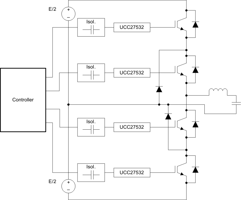 Figure 7-3 Using UCC27532 Drivers in an Inverter
SLUSBD9A February 2013 – September 2024 UCC27532
PRODUCTION DATA
 Figure 7-1 Driving IGBT Without Negative Bias
 Figure 7-2 Driving IGBT With 13-V Negative Turn-Off Bias
 Figure 7-3 Using UCC27532 Drivers in an Inverter