SLUSBU9I March   2014  ā€“ August 2024 BQ2970 , BQ2971 , BQ2972 , BQ2973

PRODUCTION DATA  

  1.   1
  2. Features
  3. Applications
  4. Description
  5. Device Comparison Table
  6. Pin Configuration and Functions
    1. 5.1 Pin Descriptions
      1. 5.1.1 Supply Input: BAT
      2. 5.1.2 Cell Negative Connection: VSS
      3. 5.1.3 Voltage Sense Node: Vā€“
      4. 5.1.4 Discharge FET Gate Drive Output: DOUT
      5. 5.1.5 Charge FET Gate Drive Output: COUT
  7. Specifications
    1. 6.1 Absolute Maximum Ratings
    2. 6.2 ESD Ratings
    3. 6.3 Recommended Operating Conditions
    4. 6.4 Thermal Information
    5. 6.5 DC Characteristics
    6. 6.6 Programmable Fault Detection Thresholds
    7. 6.7 Programmable Fault Detection Timer Ranges
    8. 6.8 Typical Characteristics
  8. Parameter Measurement Information
    1. 7.1 Timing Charts
    2. 7.2 Test Circuits
    3. 7.3 Test Circuit Diagrams
  9. Detailed Description
    1. 8.1 Overview
    2. 8.2 Functional Block Diagram
    3. 8.3 Feature Description
    4. 8.4 Device Functional Modes
      1. 8.4.1 Normal Operation
      2. 8.4.2 Overcharge Status
      3. 8.4.3 Over-Discharge Status
      4. 8.4.4 Discharge Overcurrent Status (Discharge Overcurrent, Load Short-Circuit)
      5. 8.4.5 Charge Overcurrent Status
      6. 8.4.6 0V Charging Function Enabled
      7. 8.4.7 0V Charging Inhibit Function
      8. 8.4.8 Delay Circuit
  10. Application and Implementation
    1. 9.1 Application Information
    2. 9.2 Typical Application
      1. 9.2.1 Design Requirements
      2. 9.2.2 Detailed Design Procedure
      3. 9.2.3 Application Performance Plots
    3. 9.3 Power Supply Recommendations
    4. 9.4 Layout
      1. 9.4.1 Layout Guidelines
      2. 9.4.2 Layout Example
  11. 10Device and Documentation Support
    1. 10.1 Related Documentation
    2. 10.2 Support Resources
    3. 10.3 Trademarks
    4. 10.4 Electrostatic Discharge Caution
    5. 10.5 Glossary
  12. 11Revision History
  13. 12Mechanical, Packaging, and Orderable Information

Delay Circuit

The detection delay timers are based from an internal clock with a frequency of 10kHz.
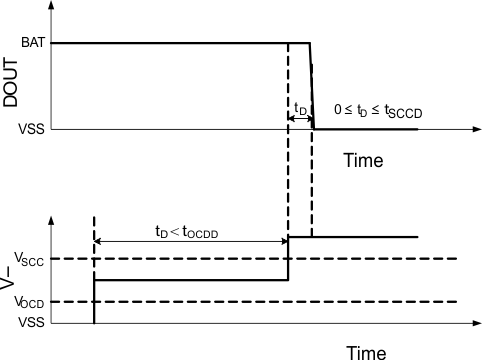
BQ2970 BQ2971 BQ2972 BQ2973 Delay CircuitFigure 8-1 Delay Circuit

If the over-discharge current is detected, but remains below the over-discharge short circuit detection threshold, the over-discharge detection conditions must be valid for a time greater than or equal to over-discharge current delay tOCCD time before the DOUT goes low to turn OFF the discharge FET. However, during any time the discharge overcurrent detection exceeds the short circuit detection threshold for a time greater than or equal to load circuit detection delay tSCCD, the DOUT pin goes low in a faster delay for protection.