SLUSCV6A April   2017  – February 2018 UCC21225A

PRODUCTION DATA.  

  1. Features
  2. Applications
  3. Description
    1.     Device Images
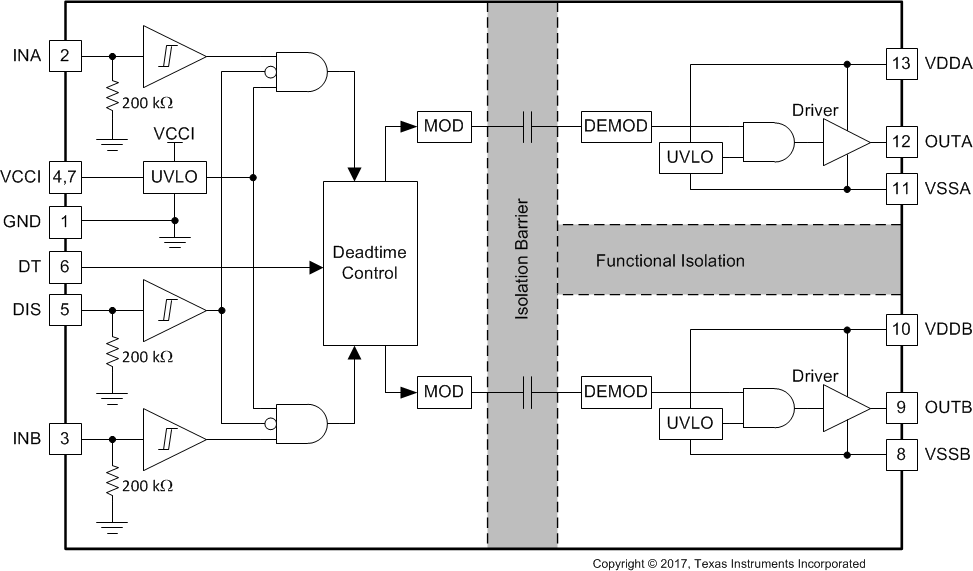
      1.      Functional Block Diagram
  4. Revision History
  5. Pin Configuration and Functions
    1.     Pin Functions
  6. Specifications
    1. 6.1  Absolute Maximum Ratings
    2. 6.2  ESD Ratings
    3. 6.3  Recommended Operating Conditions
    4. 6.4  Thermal Information
    5. 6.5  Power Ratings
    6. 6.6  Insulation Specifications
    7. 6.7  Safety-Related Certifications
    8. 6.8  Safety-Limiting Values
    9. 6.9  Electrical Characteristics
    10. 6.10 Switching Characteristics
    11. 6.11 Insulation Characteristics and Thermal Derating Curves
    12. 6.12 Typical Characteristics
  7. Parameter Measurement Information
    1. 7.1 Propagation Delay and Pulse Width Distortion
    2. 7.2 Rising and Falling Time
    3. 7.3 Input and Disable Response Time
    4. 7.4 Programable Dead Time
    5. 7.5 Power-up UVLO Delay to OUTPUT
    6. 7.6 CMTI Testing
  8. Detailed Description
    1. 8.1 Overview
    2. 8.2 Functional Block Diagram
    3. 8.3 Feature Description
      1. 8.3.1 VDD, VCCI, and Under Voltage Lock Out (UVLO)
      2. 8.3.2 Input and Output Logic Table
      3. 8.3.3 Input Stage
      4. 8.3.4 Output Stage
      5. 8.3.5 Diode Structure in UCC21225A
    4. 8.4 Device Functional Modes
      1. 8.4.1 Disable Pin
      2. 8.4.2 Programmable Dead Time (DT) Pin
        1. 8.4.2.1 Tying the DT Pin to VCC
        2. 8.4.2.2 DT Pin Left Open or Connected to a Programming Resistor between DT and GND Pins
  9. Application and Implementation
    1. 9.1 Application Information
    2. 9.2 Typical Application
      1. 9.2.1 Design Requirements
      2. 9.2.2 Detailed Design Procedure
        1. 9.2.2.1 Designing INA/INB Input Filter
        2. 9.2.2.2 Select External Bootstrap Diode and Series Resistor
        3. 9.2.2.3 Gate Driver Output Resistor
        4. 9.2.2.4 Estimate Gate Driver Power Loss
        5. 9.2.2.5 Estimating Junction Temperature
        6. 9.2.2.6 Selecting VCCI, VDDA/B Capacitor
          1. 9.2.2.6.1 Selecting a VCCI Capacitor
          2. 9.2.2.6.2 Selecting a VDDA (Bootstrap) Capacitor
          3. 9.2.2.6.3 Select a VDDB Capacitor
        7. 9.2.2.7 Dead Time Setting Guidelines
        8. 9.2.2.8 Application Circuits with Output Stage Negative Bias
      3. 9.2.3 Application Curves
  10. 10Power Supply Recommendations
  11. 11Layout
    1. 11.1 Layout Guidelines
    2. 11.2 Layout Example
  12. 12Device and Documentation Support
    1. 12.1 Documentation Support
      1. 12.1.1 Related Documentation
    2. 12.2 Certifications
      1. 12.2.1 Receiving Notification of Documentation Updates
    3. 12.3 Community Resources
    4. 12.4 Trademarks
    5. 12.5 Electrostatic Discharge Caution
    6. 12.6 Glossary
  13. 13Mechanical, Packaging, and Orderable Information

Functional Block Diagram

UCC21225A block_SLUSCV6.gif