SLUSD04C july   2018  – april 2023 BQ25150

PRODUCTION DATA  

  1. Features
  2. Applications
  3. Description
  4. Revision History
  5. Description (continued)
  6. Device Key Default Settings
  7. Pin Configuration and Functions
  8. Specifications
    1. 8.1 Absolute Maximum Ratings
    2. 8.2 ESD Ratings
    3. 8.3 Recommended Operating Conditions
    4. 8.4 Thermal Information
    5. 8.5 Electrical Characteristics
    6. 8.6 Timing Requirements
    7. 8.7 Typical Characteristics
  9. Detailed Description
    1. 9.1 Overview
    2. 9.2 Functional Block Diagram
    3. 9.3 Feature Description
      1. 9.3.1  Linear Charger and Power Path
        1. 9.3.1.1 Battery Charging Process
          1. 9.3.1.1.1 Pre-Charge
          2. 9.3.1.1.2 Fast Charge
          3. 9.3.1.1.3 Pre-Charge to Fast Charge Transitions and Charge Current Ramping
          4. 9.3.1.1.4 Termination
        2. 9.3.1.2 JEITA and Battery Temperature Dependent Charging
        3. 9.3.1.3 Input Voltage Based Dynamic Power Management (VINDPM) and Dynamic Power Path Management (DPPM)
        4. 9.3.1.4 Battery Supplement Mode
      2. 9.3.2  Protection Mechanisms
        1. 9.3.2.1 Input Over-Voltage Protection
        2. 9.3.2.2 Safety Timer and I2C Watchdog Timer
        3. 9.3.2.3 Thermal Protection and Thermal Charge Current Foldback
        4. 9.3.2.4 Battery Short and Over Current Protection
        5. 9.3.2.5 PMID Short Circuit
        6. 9.3.2.6 Maximum Allowable Charging Current (IMAX)
      3. 9.3.3  ADC
        1. 9.3.3.1 ADC Operation in Active Battery Mode and Low Power Mode
        2. 9.3.3.2 ADC Operation When VIN Present
        3. 9.3.3.3 ADC Measurements
        4. 9.3.3.4 ADC Programmable Comparators
      4. 9.3.4  VDD LDO
      5. 9.3.5  Load Switch / LDO Output and Control
      6. 9.3.6  PMID Power Control
      7. 9.3.7  MR Wake and Reset Input
        1. 9.3.7.1 MR Wake or Short Button Press Functions
        2. 9.3.7.2 MR Reset or Long Button Press Functions
      8. 9.3.8  14-Second Watchdog for HW Reset
      9. 9.3.9  Faults Conditions and Interrupts ( INT)
        1. 9.3.9.1 Flags and Fault Condition Response
      10. 9.3.10 Power Good ( PG) Pin
      11. 9.3.11 External NTC Monitoring (TS)
        1. 9.3.11.1 TS Thresholds
      12. 9.3.12 External NTC Monitoring (ADCIN)
      13. 9.3.13 I2C Interface
        1. 9.3.13.1 F/S Mode Protocol
    4. 9.4 Device Functional Modes
      1. 9.4.1 Ship Mode
      2. 9.4.2 Low Power
      3. 9.4.3 Active Battery
      4. 9.4.4 Charger/Adapter Mode
      5. 9.4.5 Power-Up/Down Sequencing
    5. 9.5 Register Map
      1. 9.5.1 I2C Registers
  10. 10Application and Implementation
    1. 10.1 Application Information
    2. 10.2 Typical Application
      1. 10.2.1 Design Requirements
      2. 10.2.2 Detailed Design Procedure
        1. 10.2.2.1 Input (IN/PMID) Capacitors
        2. 10.2.2.2 VDD, LDO Input and Output Capacitors
        3. 10.2.2.3 TS
        4. 10.2.2.4 IMAX Selection
        5. 10.2.2.5 Recommended Passive Components
      3. 10.2.3 Application Curves
  11. 11Power Supply Recommendations
  12. 12Layout
    1. 12.1 Layout Guidelines
    2. 12.2 Layout Example
  13. 13Device and Documentation Support
    1. 13.1 Device Support
      1. 13.1.1 Third-Party Products Disclaimer
    2. 13.2 Documentation Support
      1. 13.2.1 Related Documentation
    3. 13.3 Receiving Notification of Documentation Updates
    4. 13.4 Support Resources
    5. 13.5 Trademarks
    6. 13.6 Electrostatic Discharge Caution
    7. 13.7 Glossary
  14. 14Mechanical, Packaging, and Orderable Information

Battery Charging Process

Figure 9-1 summarizes the charging process of the BQ25150 charger.

GUID-18B0F267-5DFD-464E-A343-C6D39D316F1B-low.gifFigure 9-1 BQ25150 Charger Flow Diagram

When a valid input source is connected (VIN > VUVLO and VBAT + VSLP < VIN < VOVP), the state of the CE pin determines whether a charge cycle is initiated. When the CE input is high and a valid input source is connected, the battery charge FET is turned off, preventing any kind of charging of the battery. A charge cycle is initiated when the CHARGE_DISABLE bit is written to 0 and CE pin in low. Table 9-1 shows the CE pin and bit priority to enable/disable charging.

Table 9-1 Charge Enable Function Through CE Pin and CE Bit
/CE PINCHARGE _DISABLE BITCHARGING
00Enabled
01Disabled
10Disabled
11Disabled

The following figure shows a typical charge cycle.
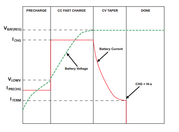
GUID-D15748E3-4F16-4EE2-B0F5-8484C7CED1C1-low.pngFigure 9-2 BQ25150 Typical Charge Cycle