SLUSD12A October 2017 – February 2018 UCC28780
PRODUCTION DATA.
- 1 Features
- 2 Applications
- 3 Description
- 4 Revision History
- 5 Pin Configuration and Functions
- 6 Specifications
-
7 Detailed Description
- 7.1 Overview
- 7.2 Functional Block Diagram
- 7.3
Detailed Pin Description
- 7.3.1 BUR Pin (Programmable Burst Mode)
- 7.3.2 FB Pin (Feedback Pin)
- 7.3.3 VDD Pin (Device Bias Supply)
- 7.3.4 REF Pin (Internal 5-V Bias)
- 7.3.5 HVG and SWS Pins
- 7.3.6 RTZ Pin (Sets Delay for Transition Time to Zero)
- 7.3.7 RDM Pin (Sets Synthesized Demagnetization Time for ZVS Tuning)
- 7.3.8 RUN Pin (Driver Enable Pin)
- 7.3.9 SET Pin
- 7.4
Device Functional Modes
- 7.4.1 Adaptive ZVS Control with Auto-Tuning
- 7.4.2 Dead-Time Optimization
- 7.4.3 Control Law across Entire Load Range
- 7.4.4 Adaptive Amplitude Modulation (AAM)
- 7.4.5 Adaptive Burst Mode (ABM)
- 7.4.6 Low Power Mode (LPM)
- 7.4.7 Standby Power Mode (SBP)
- 7.4.8 Startup Sequence
- 7.4.9 Survival Mode of VDD
- 7.4.10 System Fault Protections
- 7.4.11 Pin Open/Short Protections
-
8 Application and Implementation
- 8.1 Application Information
- 8.2
Typical Application Circuit
- 8.2.1 Design Requirements
- 8.2.2 Detailed Design Procedure
- 8.2.3 Application Curves
- 9 Power Supply Recommendations
- 10Layout
- 11Device and Documentation Support
- 12Mechanical, Packaging, and Orderable Information
8.2.3 Application Curves
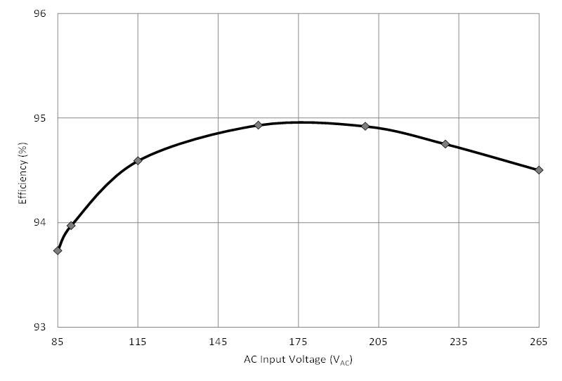
Figure 42. Full-Load Efficiency in Universal AC Line
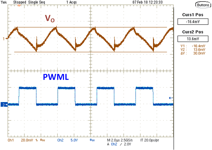
Figure 44. Output Voltage Ripple at VIN = 115 VRMS and IO = 2.25 A
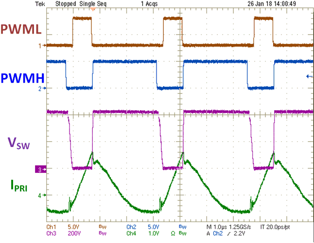
Figure 46. AAM Waveforms at VIN = 230 VRMS and IO = 2.25 A
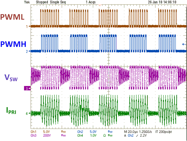
Figure 48. ABM Waveforms at VIN = 115 VRMS and IO = 0.9 A
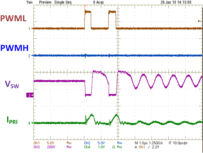
Figure 50. SBP Waveforms at VIN = 115 VRMS and IO = 0 A
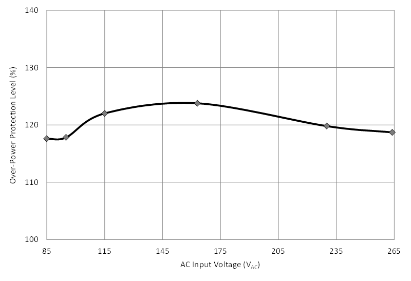
Figure 52. OPP Level in Universal AC Line
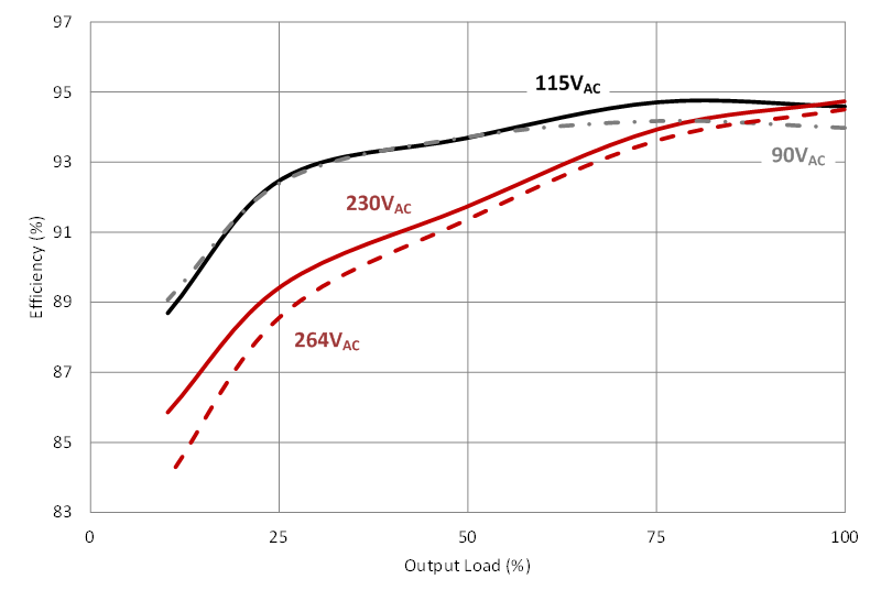
Figure 43. Light-Load Efficiency in Universal AC Line
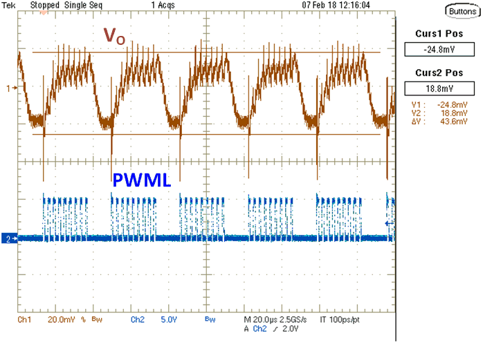
Figure 45. Output Voltage Ripple at VIN = 115 VRMS and IO = 0.9 A
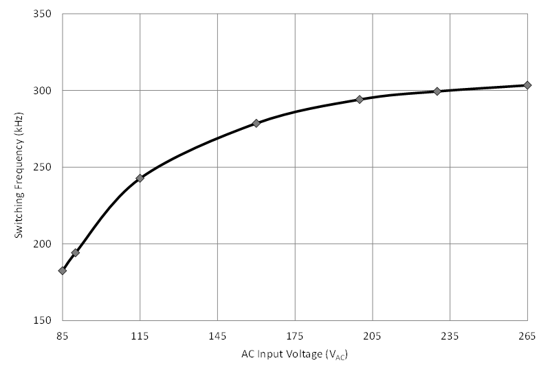
Figure 47. Switching Frequency in Universal Line and IO = 2.25 A
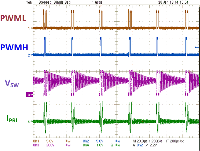
Figure 49. ABM Waveforms at VIN = 115 VRMS and IO = 0.2 A
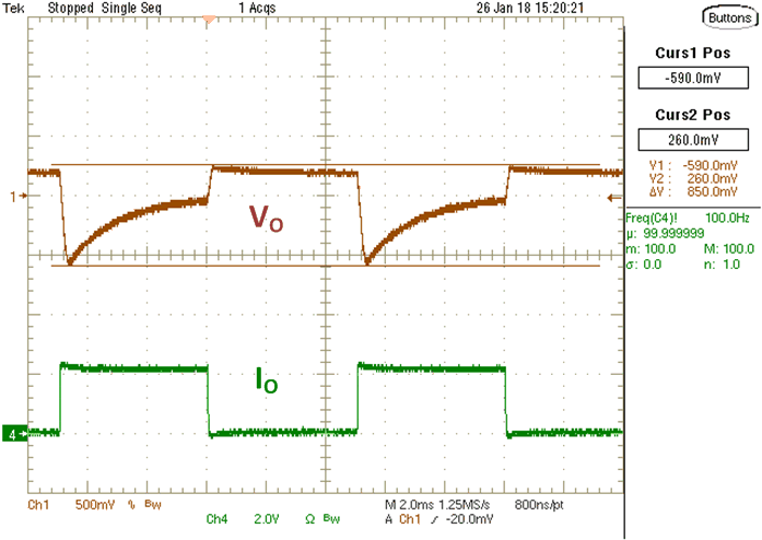
Figure 51. Load Transient between 0 A to 2.25 A at VIN = 115 VRMS
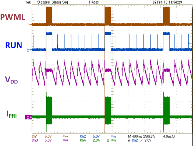
Figure 53. Fault Delay Recovery of OPP