SLUSD12A October 2017 – February 2018 UCC28780
PRODUCTION DATA.
- 1 Features
- 2 Applications
- 3 Description
- 4 Revision History
- 5 Pin Configuration and Functions
- 6 Specifications
-
7 Detailed Description
- 7.1 Overview
- 7.2 Functional Block Diagram
- 7.3
Detailed Pin Description
- 7.3.1 BUR Pin (Programmable Burst Mode)
- 7.3.2 FB Pin (Feedback Pin)
- 7.3.3 VDD Pin (Device Bias Supply)
- 7.3.4 REF Pin (Internal 5-V Bias)
- 7.3.5 HVG and SWS Pins
- 7.3.6 RTZ Pin (Sets Delay for Transition Time to Zero)
- 7.3.7 RDM Pin (Sets Synthesized Demagnetization Time for ZVS Tuning)
- 7.3.8 RUN Pin (Driver Enable Pin)
- 7.3.9 SET Pin
- 7.4
Device Functional Modes
- 7.4.1 Adaptive ZVS Control with Auto-Tuning
- 7.4.2 Dead-Time Optimization
- 7.4.3 Control Law across Entire Load Range
- 7.4.4 Adaptive Amplitude Modulation (AAM)
- 7.4.5 Adaptive Burst Mode (ABM)
- 7.4.6 Low Power Mode (LPM)
- 7.4.7 Standby Power Mode (SBP)
- 7.4.8 Startup Sequence
- 7.4.9 Survival Mode of VDD
- 7.4.10 System Fault Protections
- 7.4.11 Pin Open/Short Protections
-
8 Application and Implementation
- 8.1 Application Information
- 8.2
Typical Application Circuit
- 8.2.1 Design Requirements
- 8.2.2 Detailed Design Procedure
- 8.2.3 Application Curves
- 9 Power Supply Recommendations
- 10Layout
- 11Device and Documentation Support
- 12Mechanical, Packaging, and Orderable Information
7.4.2 Dead-Time Optimization
The dead-time optimizer in Figure 19 controls the two dead-times: the dead-time between PWMH falling edge and PWML rising edge (tZ), as well as the dead-time between PWML falling edge and PWMH rising edge (tD(PWML-H)).
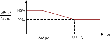
The adaptive control law for tZ of UCC28780 utilizes the line feed-forward signal to extend tZ as VBULK reduces, as shown in Figure 21. The VS pin senses VBULK through the auxiliary winding voltage (VAUX) when the low-side switch (QL) is on. The auxiliary winding creates a line-sensing current (IVSL) out of the VS pin flowing through the upper resistor of the voltage divider on VS pin (RVS1). Minimum tZ (tZ(MIN)) is set at VBULK(MAX) through the RTZ pin. When IVSL is lower than 666 μA, tZ linearly increases and the maximum tZ extension is 140% of tZ(MIN).
 Figure 21. tZ Control Optimized for Wide Input Voltage Range
The control law for tD(PWML-H) of UCC28780 is programmable based on the SET pin voltage. When VSET = 0 V, a fixed delay around 40 ns is used to fit a GaN-based ACF with a fast dV/dt on the VSW rising edge. With VSET = 5 V, the dead-time optimization is enabled to intelligently adapt to the effect of nonlinear junction capacitance of Si MOSFETs on the dV/dt of VSW rising edge. The high capacitance region of the COSS curve for the Si QL creates a shallow ramping on VSW after PWML turns off. When COSS of Si QL moves to the low capacitance region with VSW increasing, VSW starts to ramp up very quickly. Since the changing slope varies with different peak magnetizing currents as output load changes, using a fixed dead-time can potentially cause hard-switching on the high-side clamp switch (QH) if the dead-time is not long enough. UCC28780 utilizes the zero crossing detect (ZCD) signal on the auxiliary-winding voltage to identify if VSW overcomes the shallow ramping, and generates a 50-ns delay (tD(VS-PWMH)) before turning on PWMH. This feature allows cycle-by-cycle dead-time adjustment to avoid hard-switching of QH, while providing fast turn-on timing for QH to minimize the body-diode conduction time.
.gif) Figure 22. tD(PWML-H) Control Optimized for GaN and Si FETs
Figure 22. tD(PWML-H) Control Optimized for GaN and Si FETs