SLUSDB2B August 2018 – October 2024 UCC28950 , UCC28951
PRODUCTION DATA
- 1
- 1 Features
- 2 Applications
- 3 Description
- 4 Pin Configuration and Functions
- 5 Specifications
-
6 Detailed Description
- 6.1 Overview
- 6.2 Functional Block Diagram
- 6.3
Feature Description
- 6.3.1 Start-Up Protection Logic
- 6.3.2 Voltage Reference (VREF)
- 6.3.3 Error Amplifier (EA+, EA–, COMP)
- 6.3.4 Soft-Start and Enable (SS/EN)
- 6.3.5 Light-Load Power Saving Features
- 6.3.6 Adaptive Delay, (Delay Between OUTA and OUTB, OUTC and OUTD (DELAB, DELCD, ADEL))
- 6.3.7 Adaptive Delay (Delay Between OUTA and OUTF, OUTB and OUTE (DELEF, ADELEF)
- 6.3.8 Minimum Pulse (TMIN)
- 6.3.9 Burst Mode
- 6.3.10 Switching Frequency Setting
- 6.3.11 Slope Compensation (RSUM)
- 6.3.12 Dynamic SR ON/OFF Control (DCM Mode)
- 6.3.13 Current Sensing (CS)
- 6.3.14 Cycle-by-Cycle Current Limit Current Protection and Hiccup Mode
- 6.3.15 Synchronization (SYNC)
- 6.3.16 Outputs (OUTA, OUTB, OUTC, OUTD, OUTE, OUTF)
- 6.3.17 Supply Voltage (VDD)
- 6.3.18 Ground (GND)
- 6.4 Device Functional Modes
-
7 Application and Implementation
- 7.1 Application Information
- 7.2
Typical Application
- 7.2.1 Design Requirements
- 7.2.2
Detailed Design Procedure
- 7.2.2.1 Power Loss Budget
- 7.2.2.2 Preliminary Transformer Calculations (T1)
- 7.2.2.3 QA, QB, QC, QD FET Selection
- 7.2.2.4 Selecting LS
- 7.2.2.5 Selecting Diodes DB and DC
- 7.2.2.6 Output Inductor Selection (LOUT)
- 7.2.2.7 Output Capacitance (COUT)
- 7.2.2.8 Select FETs QE and QF
- 7.2.2.9 Input Capacitance (CIN)
- 7.2.2.10 Current Sense Network (CT, RCS, R7, DA)
- 7.2.3 Application Curves
- 7.3 Power Supply Recommendations
- 7.4 Layout
- 8 Device and Documentation Support
- 9 Revision History
- 10Mechanical, Packaging, and Orderable Information
5.7 Dissipation Ratings
over operating free-air temperature range (unless otherwise noted)
| PACKAGE | DERATING FACTOR | POWER RATING | ||
|---|---|---|---|---|
| ABOVE TA = 25°C | TA < 25°C | TA = 70°C | TA = 85°C | |
| PW | 10.7mW/°C | 1.07W | 0.59W | 0.429W |

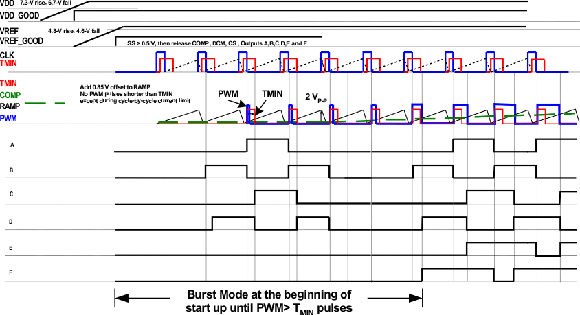
No output delay
shown, COMP-to-RAMP offset not included.
There is no pulse
on OUTE during burst mode at start-up. Two falling edge PWM pulses are required
before enabling the synchronous rectifier outputs. Narrower pulse widths (less
than 50% duty cycle) may be observed in the 1st OUTD pulse of a burst. The user
must design the bootstrap capacitor charging circuit of the gate driver device
so that the first OUTC pulse is transmitted to the MOSFET gate in all cases.
Transformer based gate driver circuits are not affected. This behavior is
described in more detail in the Gate Drive Outputs on the UCC28950
and UCC2895x During Burst Mode Operation
(SLAU787) application note.
Figure 5-1 UCC2895x Start-Up Timing
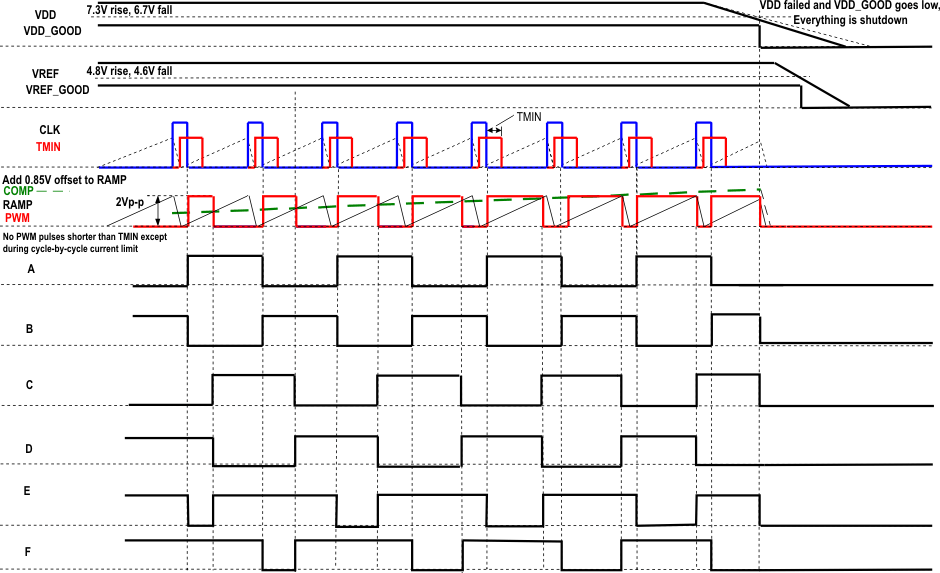
No output delay
shown, COMP-to-RAMP offset not included.
Figure 5-2 UCC2895x Steady-State and Shutdown Timing Diagram