SLUSDC0D October   2018  – November 2024 UCC21530

PRODUCTION DATA  

  1.   1
  2. Features
  3. Applications
  4. Description
  5. Pin Configuration and Functions
  6. Specifications
    1. 5.1  Absolute Maximum Ratings
    2. 5.2  ESD Ratings
    3. 5.3  Recommended Operating Conditions
    4. 5.4  Thermal Information
    5. 5.5  Power Ratings
    6. 5.6  Insulation Specifications
    7. 5.7  Safety Limiting Values
    8. 5.8  Electrical Characteristics
    9. 5.9  Timing Requirements
    10. 5.10 Switching Characteristics
    11. 5.11 Insulation Characteristics Curves
    12. 5.12 Typical Characteristics
  7. Parameter Measurement Information
    1. 6.1 Propagation Delay and Pulse Width Distortion
    2. 6.2 Rising and Falling Time
    3. 6.3 Input and Enable Response Time
    4. 6.4 Programable Dead Time
    5. 6.5 Power-Up UVLO Delay to OUTPUT
    6. 6.6 CMTI Testing
  8. Detailed Description
    1. 7.1 Overview
    2. 7.2 Functional Block Diagram
    3. 7.3 Feature Description
      1. 7.3.1 VDD, VCCI, and Under Voltage Lock Out (UVLO)
      2. 7.3.2 Input and Output Logic Table
      3. 7.3.3 Input Stage
      4. 7.3.4 Output Stage
      5. 7.3.5 Diode Structure in UCC21530-Q1
    4. 7.4 Device Functional Modes
      1. 7.4.1 Enable Pin
      2. 7.4.2 Programmable Dead Time (DT) Pin
        1. 7.4.2.1 DT Pin Tied to VCC
        2. 7.4.2.2 DT Pin Connected to a Programming Resistor between DT and GND Pins
  9. Application and Implementation
    1. 8.1 Application Information
    2. 8.2 Typical Application
      1. 8.2.1 Design Requirements
      2. 8.2.2 Detailed Design Procedure
        1. 8.2.2.1 Designing INA/INB Input Filter
        2. 8.2.2.2 Select Dead Time Resistor and Capacitor
        3. 8.2.2.3 Gate Driver Output Resistor
        4. 8.2.2.4 Estimate Gate Driver Power Loss
        5. 8.2.2.5 Estimating Junction Temperature
        6. 8.2.2.6 Selecting VCCI, VDDA/B Capacitor
          1. 8.2.2.6.1 Selecting a VCCI Capacitor
        7. 8.2.2.7 Other Application Example Circuits
      3. 8.2.3 Application Curves
  10. Power Supply Recommendations
  11. 10Layout
    1. 10.1 Layout Guidelines
      1. 10.1.1 Component Placement Considerations
      2. 10.1.2 Grounding Considerations
      3. 10.1.3 High-Voltage Considerations
      4. 10.1.4 Thermal Considerations
    2. 10.2 Layout Example
  12. 11Device and Documentation Support
    1. 11.1 Third-Party Products Disclaimer
    2. 11.2 Documentation Support
      1. 11.2.1 Related Documentation
    3. 11.3 Receiving Notification of Documentation Updates
    4. 11.4 Support Resources
    5. 11.5 Trademarks
    6. 11.6 Glossary
  13. 12Revision History
  14. 13Mechanical, Packaging, and Orderable Information

Typical Characteristics

VDDA = VDDB = 15V (8V and 12V UVLO variants) , VCCI = 3.3 V, TA = 25°C, No load. (unless otherwise noted)

UCC21530 Per
                        Channel Current Consumption vs Frequency
No load
Figure 5-4 Per Channel Current Consumption vs Frequency
UCC21530 Per
                        Channel Current Consumption (IVDDA/B) vs
                        Frequency
                        (10-nF Load, VDD=15
                            or 25V)
Figure 5-6 Per Channel Current Consumption (IVDDA/B) vs Frequency (10-nF Load, VDD=15 or 25V)
UCC21530 Per
                        Channel (IVDDA/B) Quiescent Supply Current vs
                        Temperature
                        (No Load, Input Low, No Switching)
Figure 5-8 Per Channel (IVDDA/B) Quiescent Supply Current vs Temperature (No Load, Input Low, No Switching)
UCC21530 Rising and Falling Times vs Load
Figure 5-10 Rising and Falling Times vs Load
UCC21530 Propagation Delay vs Temperature
Figure 5-12 Propagation Delay vs Temperature
UCC21530 Pulse
                        Width Distortion vs Temperature
Figure 5-14 Pulse Width Distortion vs Temperature
UCC21530 Propagation Delay Matching (tDM) vs Temperature
Figure 5-16 Propagation Delay Matching (tDM) vs Temperature
UCC21530 8-V
                        UVLO Threshold vs Temperature
Figure 5-18 8-V UVLO Threshold vs Temperature
UCC21530 12-V
                        UVLO Threshold vs Temperature
Figure 5-20 12-V UVLO Threshold vs Temperature
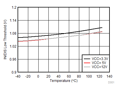
UCC21530 INA/B/EN
                        Low Threshold
Figure 5-22 INA/B/EN Low Threshold
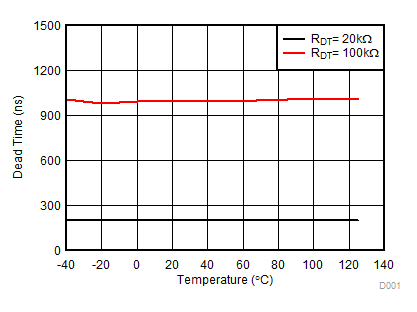
UCC21530 Dead
                        Time vs Temperature
Figure 5-24 Dead Time vs Temperature
UCC21530 Per
                        Channel Current Consumption (IVDDA/B) vs
                        Frequency
                        (1-nF Load, VDD=15V
                            or 25V)
Figure 5-5 Per Channel Current Consumption (IVDDA/B) vs Frequency (1-nF Load, VDD=15V or 25V)
UCC21530 Per
                        Channel (IVDDA/B) Supply Current vs
                        Temperature
                        (No Load, Different Switching Frequencies)
Figure 5-7 Per Channel (IVDDA/B) Supply Current vs Temperature (No Load, Different Switching Frequencies)
UCC21530 IVCCI Quiescent Supply Current vs
                        Temperature
                        (No Load, Input Low, No Switching)
Figure 5-9 IVCCI Quiescent Supply Current vs Temperature (No Load, Input Low, No Switching)
UCC21530 Output Resistance vs Temperature
Figure 5-11 Output Resistance vs Temperature
UCC21530 Propagation Delay vs VCCI
Figure 5-13 Propagation Delay vs VCCI
UCC21530 Propagation Delay Matching (tDM) vs VDD
Figure 5-15 Propagation Delay Matching (tDM) vs VDD
UCC21530 8-V
                        UVLO Hysteresis vs Temperature
Figure 5-17 8-V UVLO Hysteresis vs Temperature
UCC21530 12-V
                        UVLO Hysteresis vs Temperature
Figure 5-19 12-V UVLO Hysteresis vs Temperature
UCC21530 INA/B/EN
                        Hysteresis vs Temperature
Figure 5-21 INA/B/EN Hysteresis vs Temperature
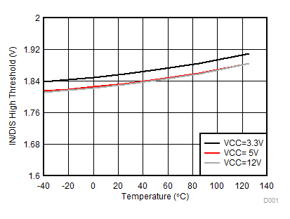
UCC21530 INA/B/EN
                        High Threshold
Figure 5-23 INA/B/EN High Threshold
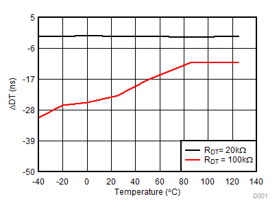
UCC21530 Dead
                        Time Matching vs Temperature
Figure 5-25 Dead Time Matching vs Temperature