SLUSDC7A March   2020  – November 2020 BQ25306

PRODUCTION DATA  

  1. Features
  2. Applications
  3. Description
  4. Revision History
  5. Description (continued)
  6. Device Comparison Table
  7. Pin Configuration and Functions
  8. Specifications
    1. 8.1 Absolute Maximum Ratings
    2. 8.2 ESD Ratings
    3. 8.3 Recommended Operating Conditions
    4. 8.4 Thermal Information
    5. 8.5 Electrical Characteristics
    6. 8.6 Timing Requirements
    7. 8.7 Typical Characteristics
  9. Detailed Description
    1. 9.1 Overview
    2. 9.2 Functional Block Diagram
    3. 9.3 Feature Description
      1. 9.3.1 Device Power Up
        1. 9.3.1.1 Power-On-Reset (POR)
        2. 9.3.1.2 REGN Regulator Power Up
        3. 9.3.1.3 Charger Power Up
        4. 9.3.1.4 Charger Enable and Disable by EN Pin
        5. 9.3.1.5 Device Unplugged from Input Source
      2. 9.3.2 Battery Charging Management
        1. 9.3.2.1 Battery Charging Profile
        2. 9.3.2.2 Precharge
        3. 9.3.2.3 Charging Termination
        4. 9.3.2.4 Battery Recharge
        5. 9.3.2.5 Charging Safety Timer
        6. 9.3.2.6 Thermistor Temperature Monitoring
      3. 9.3.3 Charging Status Indicator (STAT)
      4. 9.3.4 Protections
        1. 9.3.4.1 Voltage and Current Monitoring
          1. 9.3.4.1.1 Input Over-Voltage Protection
          2. 9.3.4.1.2 Input Voltage Dynamic Power Management (VINDPM)
          3. 9.3.4.1.3 Input Current Limit
          4. 9.3.4.1.4 Cycle-by-Cycle Current Limit
        2. 9.3.4.2 Thermal Regulation and Thermal Shutdown
        3. 9.3.4.3 Battery Protection
          1. 9.3.4.3.1 Battery Over-Voltage Protection (VBAT_OVP)
          2. 9.3.4.3.2 Battery Short Circuit Protection
        4. 9.3.4.4 ICHG Pin Open and Short Protection
    4. 9.4 Device Functional Modes
      1. 9.4.1 Disable Mode, HiZ Mode, Sleep Mode, Charge Mode, Termination Mode, and Fault Mode
  10. 10Application and Implementation
    1. 10.1 Application Information
    2. 10.2 Typical Applications
      1. 10.2.1 Typical Application
        1. 10.2.1.1 Design Requirements
        2. 10.2.1.2 Detailed Design Procedure
          1. 10.2.1.2.1 Charge Voltage Settings
          2. 10.2.1.2.2 Charge Current Setting
          3. 10.2.1.2.3 Inductor Selection
          4. 10.2.1.2.4 Input Capacitor
          5. 10.2.1.2.5 Output Capacitor
        3. 10.2.1.3 Application Curves
      2. 10.2.2 Typical Application with External Power Path
        1. 10.2.2.1 Design Requirements
      3. 10.2.3 Typical Application with MCU Programmable Charge Current
        1. 10.2.3.1 Design Requirements
  11. 11Power Supply Recommendations
  12. 12Layout
    1. 12.1 Layout Guidelines
    2. 12.2 Layout Example
  13. 13Device and Documentation Support
    1. 13.1 Device Support
      1. 13.1.1 Third-Party Products Disclaimer
    2. 13.2 Documentation Support
      1. 13.2.1 Related Documentation
    3. 13.3 Receiving Notification of Documentation Updates
    4. 13.4 Support Resources
    5. 13.5 Trademarks
    6. 13.6 Electrostatic Discharge Caution
    7. 13.7 Glossary
  14. 14Mechanical, Packaging, and Orderable Information
Inductor Selection

The 1.2-MHz switching frequency allows the use of small inductor and capacitor values. Inductance value is selected based on maximum input voltage VVBUS_MAX in applications. 1-µH inductor is recommended if VVBUS_MAX < 6.2V and 2.2-µH inductor is recommended if VVBUS_MAX > 6.2V for either 1-cell or 2-cell battery charge. An inductor saturation current ISATshould be higher than the charging curren ICHG plus half the ripple current IRIPPLE:

Equation 3. ISAT ≥ ICHG + (1/2) IRIPPLE

The inductor ripple current IRIPPLE depends on the input voltage (VVBUS), the duty cycle (D = VBAT/VVBUS), the switching frequency (fS) and the inductance (L).

Equation 4. GUID-58D6EC74-40EE-4838-8D55-16FFA87707B6-low.gif

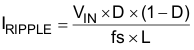
The maximum inductor ripple current occurs when the duty cycle (D) is 0.5 or approximately 0.5.