-
TPS560430-Q1 SIMPLE SWITCHER 4-V to 36-V, 600-mA Synchronous Buck Converter
- 1 Features
- 2 Applications
- 3 Description
- 4 Revision History
- 5 Device Comparison Table
- 6 Pin Configuration and Functions
- 7 Specifications
- 8 Detailed Description
- 9 Application and Implementation
- 10Power Supply Recommendations
- 11Layout
- 12Device and Documentation Support
- 13Mechanical, Packaging, and Orderable Information
- IMPORTANT NOTICE
TPS560430-Q1 SIMPLE SWITCHER 4-V to 36-V, 600-mA Synchronous Buck Converter
1 Features
- Qualified for automotive applications
- AEC-Q100 Qualified
- Temperature grade 1: –40°C to 125°C ambient operating temperature range
- ESD HBM classification level 2
- ESD CDM classification level C5 - Configured for rugged automotive applications
- Input voltage range: 4 V to 36 V
- 600-mA continuous output current
- Minimum switching-on time: 60 ns
- Fixed 2.1MHz frequency
- 98% maximum duty cycle
- Support startup with pre-biased output
- Short circuit protection with hiccup mode
- ±0.5% tolerance voltage reference at room temperature
- Precision enable
- Small solution size and ease of use
- Integrated synchronous rectification
- Internal compensation for ease of use
- SOT-23-6 package
- Two modes in pin-to-pin compatible package
- PFM and forced PWM (FPWM) options
- Create a custom design using the TPS560430-Q1 with the WEBENCH® Power Designer
2 Applications
- Camera
- On-board charger
- Automotive head unit
- USB charger
- General purpose wide VIN power supplies
3 Description
The TPS560430-Q1 is a wide-VIN, easy to use synchronous buck converter capable of driving up to 600-mA load current. With a wide input range of 4 V to 36 V, the device is suitable for a wide range of automotive applications for power conditioning from an unregulated source.
TPS560430-Q1 operates at 2.1-MHz switching frequency to support use of relatively small inductors for an optimized solution size. It has Eco-mode version to realize high efficiency at light load and FPWM version to achieve constant frequency, small output voltage ripple over the full load range. Soft-start and compensation circuits are implemented internally which allows the device to be used with minimum external components.
The device has built-in protection features, such as cycle-by-cycle current limit, hiccup mode short-circuit protection, and thermal shutdown in case of excessive power dissipation. The TPS560430-Q1 is available in SOT-23-6 package.
Device Information (1)
| PART NUMBER | PACKAGE | BODY SIZE (NOM) |
|---|---|---|
| TPS560430-Q1 | SOT-23-6 | 2.90 mm × 1.60 mm |
- For all available packages, see the orderable addendum at the end of the data sheet.
Device Images
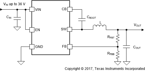
Simplified Schematic

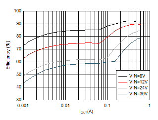
Efficiency vs Output Current
VOUT = 5 V, 2100 kHz, PFM
