SLUSDF5A January   2019  – August 2019 TPS560430-Q1

PRODUCTION DATA.  

  1. Features
  2. Applications
  3. Description
    1.     Device Images
      1.      Simplified Schematic
      2.      Efficiency vs Output Current VOUT = 5 V, 2100 kHz, PFM
  4. Revision History
  5. Device Comparison Table
  6. Pin Configuration and Functions
    1.     Pin Functions
  7. Specifications
    1. 7.1 Absolute Maximum Ratings
    2. 7.2 ESD Ratings
    3. 7.3 Recommended Operating Conditions
    4. 7.4 Thermal Information
    5. 7.5 Electrical Characteristics
    6. 7.6 Timing Requirements
    7. 7.7 Switching Characteristics
    8. 7.8 Typical Characteristics
  8. Detailed Description
    1. 8.1 Overview
    2. 8.2 Functional Block Diagram
    3. 8.3 Feature Description
      1. 8.3.1 Fixed Frequency Peak Current Mode Control
      2. 8.3.2 Adjustable Output Voltage
      3. 8.3.3 Enable
      4. 8.3.4 Minimum ON-Time, Minimum OFF-Time and Frequency Foldback
      5. 8.3.5 Bootstrap Voltage
      6. 8.3.6 Over Current and Short Circuit Protection
      7. 8.3.7 Soft Start
      8. 8.3.8 Thermal Shutdown
    4. 8.4 Device Functional Modes
      1. 8.4.1 Shutdown Mode
      2. 8.4.2 Active Mode
      3. 8.4.3 CCM Mode
      4. 8.4.4 Light-Load Operation (PFM Version)
      5. 8.4.5 Light-Load Operation (FPWM Version)
  9. Application and Implementation
    1. 9.1 Application Information
    2. 9.2 Typical Application
      1. 9.2.1 Design Requirements
      2. 9.2.2 Detailed Design Procedure
        1. 9.2.2.1 Custom Design With WEBENCH® Tools
        2. 9.2.2.2 Output Voltage Set-Point
        3. 9.2.2.3 Switching Frequency
        4. 9.2.2.4 Inductor Selection
        5. 9.2.2.5 Output Capacitor Selection
        6. 9.2.2.6 Input Capacitor Selection
        7. 9.2.2.7 Bootstrap Capacitor
        8. 9.2.2.8 Under Voltage Lockout Set-Point
      3. 9.2.3 Application Curves
  10. 10Power Supply Recommendations
  11. 11Layout
    1. 11.1 Layout Guidelines
      1. 11.1.1 Compact Layout for EMI Reduction
      2. 11.1.2 Feedback Resistors
    2. 11.2 Layout Example
  12. 12Device and Documentation Support
    1. 12.1 Device Support
      1. 12.1.1 Development Support
        1. 12.1.1.1 Custom Design With WEBENCH® Tools
    2. 12.2 Documentation Support
      1. 12.2.1 Related Documentation
    3. 12.3 Receiving Notification of Documentation Updates
    4. 12.4 Community Resources
    5. 12.5 Trademarks
    6. 12.6 Electrostatic Discharge Caution
    7. 12.7 Glossary
  13. 13Mechanical, Packaging, and Orderable Information

Application Curves

Unless otherwise specified the following conditions apply: VIN = 12 V, VOUT = 5 V, fSW = 2.1 MHz, L = 8.2 µH, COUT = 10 µF, TA = 25 °C
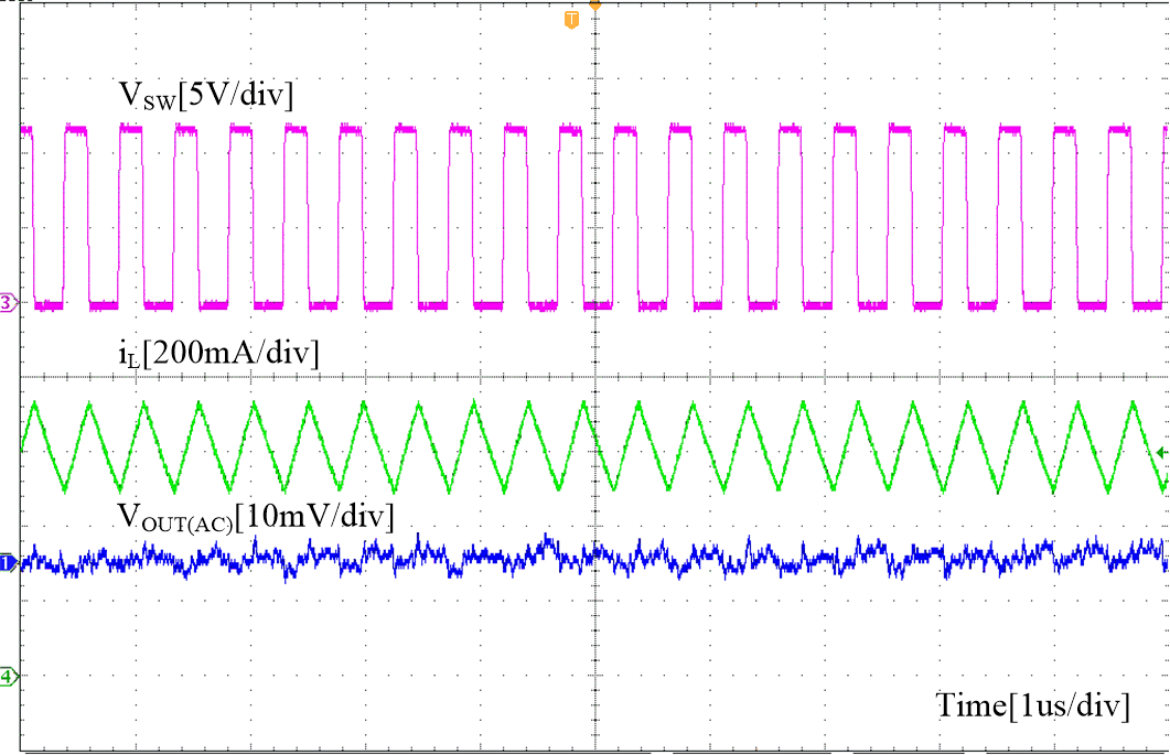
TPS560430-Q1 SLUSDF5-Fig-16-Ripple-at-No-Load.gif
IOUT = 0 mA FPWM Version
Figure 16. Ripple at No Load
TPS560430-Q1 SLUSDF5-start-up(2).gif
IOUT = 600 mA FPWM Version
Figure 18. Start Up by VIN
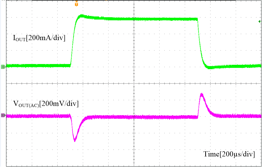
TPS560430-Q1 SLUSDF5-Fig-20-Load-Transient.gif
IOUT = 0 to 600 mA, 100 mA / µs FPWM Version
Figure 20. Load Transient
TPS560430-Q1 SLUSDF5-hiccup-to-recover(2).gif
IOUT = short to 0 mA FPWM Version
Figure 22. Short Recovery
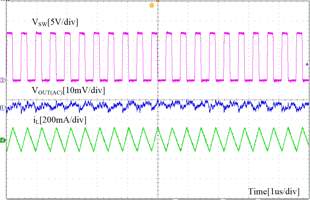
TPS560430-Q1 SLUSDF5-Fig-17-Ripple-at-Full-Load.gif
IOUT = 600 mA FPWM Version
Figure 17. Ripple at Full Load
TPS560430-Q1 SLUSDF5-EN-Start-up(2).gif
IOUT = 600 mA FPWM Version
Figure 19. Start-Up by EN
TPS560430-Q1 SLUSDF5-short-to-hiccup(2).gif
IOUT = 0 mA to short FPWM Version
Figure 21. Short Protection