SLUSDG3F August 2018 – September 2024 UCC21530-Q1
PRODUCTION DATA
- 1
- 1 Features
- 2 Applications
- 3 Description
- 4 Pin Configuration and Functions
-
5 Specifications
- 5.1 Absolute Maximum Ratings
- 5.2 ESD Ratings (Automotive)
- 5.3 Recommended Operating Conditions
- 5.4 Thermal Information
- 5.5 Power Ratings
- 5.6 Insulation Specifications
- 5.7 Safety Limiting Values
- 5.8 Electrical Characteristics
- 5.9 Timing Requirements
- 5.10 Switching Characteristics
- 5.11 Insulation Characteristics Curves
- 5.12 Typical Characteristics
- 6 Parameter Measurement Information
- 7 Detailed Description
-
8 Application and Implementation
- 8.1 Application Information
- 8.2
Typical Application
- 8.2.1 Design Requirements
- 8.2.2 Detailed Design Procedure
- 8.2.3 Application Curves
- 9 Power Supply Recommendations
- 10Layout
- 11Device and Documentation Support
- 12Revision History
- 13Mechanical, Packaging, and Orderable Information
6.5 Power-Up UVLO Delay to OUTPUT
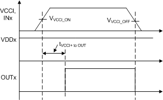
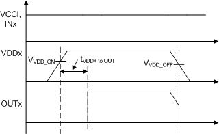
Whenever the supply voltage VCCI crosses from below the falling threshold VVCCI_OFF to above the rising threshold VVCCI_ON, and whenever the supply voltage VDDx crosses from below the falling threshold VVDDx_OFF to above the rising threshold VVDDx_ON, there is a delay before the outputs begin responding to the inputs. For VCCI UVLO this delay is defined as tVCCI+ to OUT, and has a maximum of 50 µs. For VDDx UVLO this delay is defined as tVDD+ to OUT, and has a maximum of 10 µs. TI recommends allowing some margin before driving input signals, to ensure the driver VCCI and VDD bias supplies are fully activated. Figure 6-5 and Figure 6-6 show the power-up UVLO delay timing diagram for VCCI and VDD.
Whenever the supply voltage VCCI crosses below the falling threshold VVCCI_OFF, or VDDx crosses below the falling threshold VVDDx_OFF, the outputs stop responding to the inputs and are held low within <2 µs. This asymmetric delay is designed to ensure safe operation during VCCI or VDDx brownouts.
 Figure 6-5 VCCI Power-Up UVLO
Delay
 Figure 6-6 VDDA/B Power-Up UVLO
Delay