SLUSE44D April 2020 – May 2024 UCC27624
PRODUCTION DATA
7.2.2.1 VDD and Undervoltage Lockout
The UCC27624 device has an internal undervoltage-lockout (UVLO) protection feature on the VDD pin supply circuit blocks. When VDD is rising and the level is still below UVLO threshold, this circuit holds the output low, regardless of the status of the inputs. The UVLO is typically 4 V with 300-mV typical hysteresis. This hysteresis prevents chatter when VDD supply voltages have noise, specifically at the lower end of the VDD operating range. UVLO hysteresis is also important to avoid any false tripping due to the bias noise generated because of fast switching transitions, where large peak currents are drawn from the bias supply bypass capacitors. The driver capability to operate at wide bias voltage range, along with good switching characteristics, is especially important in driving emerging power semiconductor devices, such as advanced low gate charge fast MOSFETs, GaN FETs, and SiC MOSFETs.
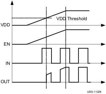
At power-up, the UCC27624 driver device output remains low until the VDD voltage reaches the UVLO rising threshold, irrespective of the state of any other input pins such as INx and ENx. After the UVLO rising threshold, the magnitude of the OUT signal rises with VDD until steady-state VDD is reached.
For the best high-speed circuit performance and to prevent noise problems because the device draws current from the VDD pin to bias all internal circuits, use two VDD bypass capacitors. Also, use surface mount, low ESR capacitors. A 0.1-μF ceramic capacitor should be located less than 1 mm from the VDD to GND pins of the gate-driver device. In addition, a larger capacitor (≥1 μF) must be connected in parallel (also as close to the driver IC as possible) to help deliver the high-current peaks required by the load. The parallel combination of capacitors presents a low impedance characteristic for the expected current levels and switching frequencies in the application.
 Figure 7-2 Power-Up
Sequence