SLUSE89C May 2023 – August 2024 UCC21550
PRODUCTION DATA
- 1
- 1 Features
- 2 Applications
- 3 Description
- 4 Pin Configuration and Functions
-
5 Specifications
- 5.1 Absolute Maximum Ratings
- 5.2 ESD Ratings
- 5.3 Recommended Operating Conditions
- 5.4 Thermal Information
- 5.5 Power Ratings
- 5.6 Insulation Specifications
- 5.7 Safety Limiting Values
- 5.8 Electrical Characteristics
- 5.9 Switching Characteristics
- 5.10 Insulation Characteristics Curves
- 5.11 Typical Characteristics
- 6 Parameter Measurement Information
- 7 Detailed Description
-
8 Application and Implementation
- 8.1 Application Information
- 8.2
Typical Application
- 8.2.1 Design Requirements
- 8.2.2
Detailed Design Procedure
- 8.2.2.1 Designing INA/INB Input Filter
- 8.2.2.2 Select External Bootstrap Diode and its Series Resistor
- 8.2.2.3 Gate Driver Output Resistor
- 8.2.2.4 Gate to Source Resistor Selection
- 8.2.2.5 Estimate Gate Driver Power Loss
- 8.2.2.6 Estimating Junction Temperature
- 8.2.2.7 Selecting VCCI, VDDA/B Capacitor
- 8.2.2.8 Dead Time Setting Guidelines
- 8.2.2.9 Application Circuits with Output Stage Negative Bias
- 8.2.3 Application Curves
- 9 Power Supply Recommendations
- 10Layout
- 11Device and Documentation Support
- 12Revision History
- 13Mechanical, Packaging, and Orderable Information
8.2 Typical Application
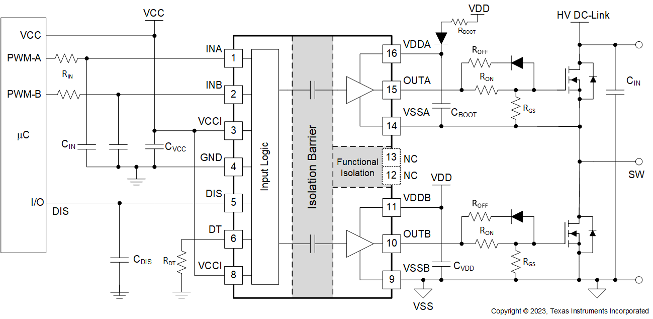
The circuit in Figure 8-1 shows a reference design with the UCC21550 driving a typical half-bridge configuration which could be used in several popular power converter topologies such as synchronous buck, synchronous boost, half-bridge/full bridge isolated topologies, and 3-phase motor drive applications.
 Figure 8-1 Typical
Application Schematic