SLUSE89C May 2023 – August 2024 UCC21550
PRODUCTION DATA
- 1
- 1 Features
- 2 Applications
- 3 Description
- 4 Pin Configuration and Functions
-
5 Specifications
- 5.1 Absolute Maximum Ratings
- 5.2 ESD Ratings
- 5.3 Recommended Operating Conditions
- 5.4 Thermal Information
- 5.5 Power Ratings
- 5.6 Insulation Specifications
- 5.7 Safety Limiting Values
- 5.8 Electrical Characteristics
- 5.9 Switching Characteristics
- 5.10 Insulation Characteristics Curves
- 5.11 Typical Characteristics
- 6 Parameter Measurement Information
- 7 Detailed Description
-
8 Application and Implementation
- 8.1 Application Information
- 8.2
Typical Application
- 8.2.1 Design Requirements
- 8.2.2
Detailed Design Procedure
- 8.2.2.1 Designing INA/INB Input Filter
- 8.2.2.2 Select External Bootstrap Diode and its Series Resistor
- 8.2.2.3 Gate Driver Output Resistor
- 8.2.2.4 Gate to Source Resistor Selection
- 8.2.2.5 Estimate Gate Driver Power Loss
- 8.2.2.6 Estimating Junction Temperature
- 8.2.2.7 Selecting VCCI, VDDA/B Capacitor
- 8.2.2.8 Dead Time Setting Guidelines
- 8.2.2.9 Application Circuits with Output Stage Negative Bias
- 8.2.3 Application Curves
- 9 Power Supply Recommendations
- 10Layout
- 11Device and Documentation Support
- 12Revision History
- 13Mechanical, Packaging, and Orderable Information
3 Description
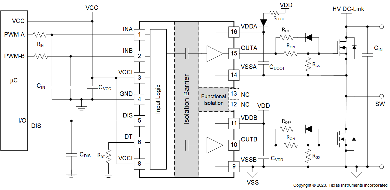
The UCC21550 is an isolated dual channel gate driver family with programmable dead time and wide temperature range. It is designed with 4A peak-source and 6A peak-sink current to drive power MOSFET, SiC, GaN, and IGBT transistors.
The UCC21550 can be configured as two low-side drivers, two high-side drivers, or a half-bridge driver. The input side is isolated from the two output drivers by a 5kVRMS isolation barrier, with a minimum of 125V/ns common-mode transient immunity (CMTI).
Protection features include: resistor programmable dead time, disable feature to shut down both outputs simultaneously, and integrated de-glitch filter that rejects input transients shorter than 5ns. All supplies have UVLO protection.
With all these advanced features, the UCC21550 device enables high efficiency, high power density, and robustness in a wide variety of power applications.
| PART NUMBER | PACKAGE(1) | REC. VDD SUPPLY MIN |
|---|---|---|
| UCC21550ADWR | DW (SOIC, 16) | 6.5V |
| UCC21550BDWR | DW (SOIC, 16) | 9.2V |
| UCC21550ADWKR | DWK (SOIC, 14) | 6.5V |
| UCC21550BDWKR | DWK (SOIC, 14) | 9.2V |
| UCC21550CDWKR | DWK (SOIC, 14) | 13.5V |
 Typical Application Schematic