SLUSEY7B December 2022 – December 2024 TPSM82816
PRODMIX
- 1
- 1 Features
- 2 Applications
- 3 Description
- 4 Device Comparison Table
- 5 Pin Configuration and Functions
- 6 Specifications
- 7 Detailed Description
- 8 Application and Implementation
- 9 Device and Documentation Support
- 10Revision History
- 11Mechanical, Packaging, and Orderable Information
8.3.1 Voltage Tracking
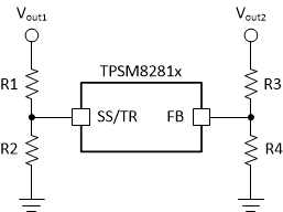
The SS/TR pin is externally driven by another voltage source to achieve output voltage tracking. The application circuit is shown in Figure 8-32. From 0 V to 0.6 V, the internal reference voltage to the internal error amplifier follows the SS/TR pin voltage. When the SS/TR pin voltage is above 0.6 V, the voltage tracking is disabled and the FB pin voltage is regulated at 0.6 V. The device achieves ratiometric, as shown in Figure 8-33 or coincidental (simultaneous) output tracking, as shown in Figure 8-33.
The R2 value must be set properly to achieve accurate voltage tracking by taking the 10-μA charging current into account. 1 kΩ or smaller is a sufficient value for R2. For decreasing SS/TR pin voltage, the device does not sink current from the output when the device is in PSM. The resulting decrease of the output voltage can be slower than the SS/TR pin voltage if the load is light.
In case both devices need to run in forced PWM mode after start-up, TI recommends to tie the MODE/SYNC pin of the secondary device to the output voltage or the power-good signal of the primary device. The TPSM8281x has a duty cycle limitation defined by the minimum on time, which can cause the secondary device to not track when the output voltage is very low. Delaying FPWM mode until the output voltage is higher operates the device in PSM mode, with improved tracking at very low output voltages
When driving the SS/TR pin with an external voltage, do not exceed the voltage rating of the SS/TR pin.
 Figure 8-32 Schematic for Output Voltage Tracking
 Figure 8-33 Ratiometric Voltage Tracking
 Figure 8-34 Coincidental Voltage Tracking