SLUSF53 August 2024 BQ2969
PRODUCTION DATA
- 1
- 1 Features
- 2 Applications
- 3 Description
- 4 Device Comparison Table
- 5 Pin Configuration and Functions
- 6 Specifications
- 7 Detailed Description
- 8 Application and Implementation
- 9 Power Supply Recommendations
- 10Layout
- 11Device and Documentation Support
- 12Revision History
- 13Mechanical, Packaging, and Orderable Information
8.2.3 Application Curves
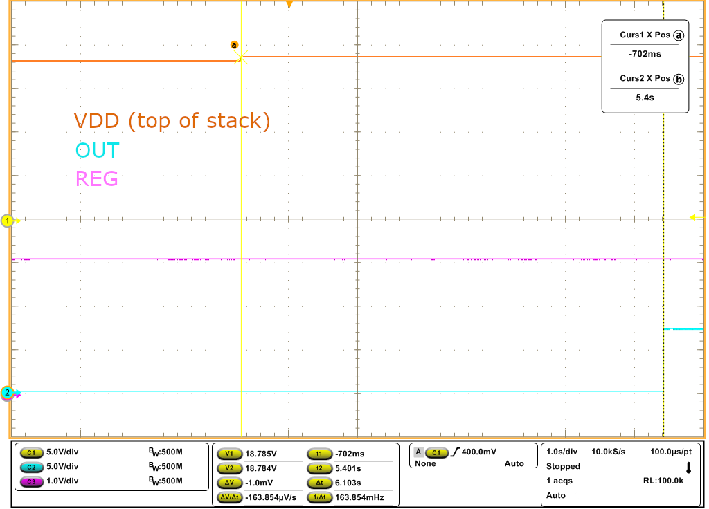
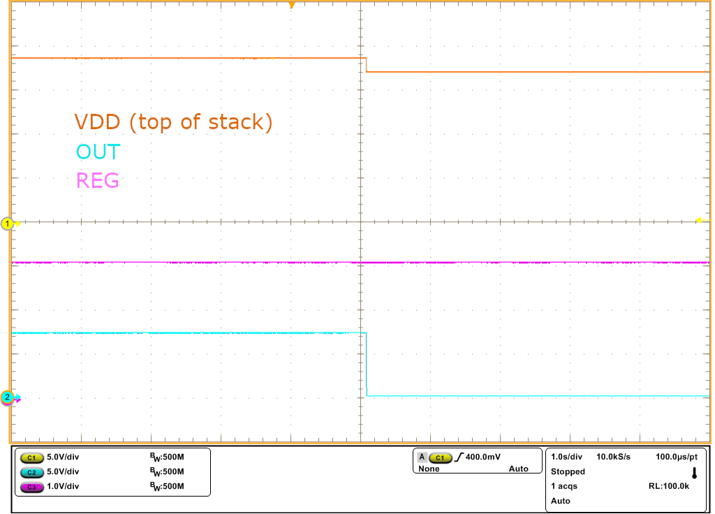
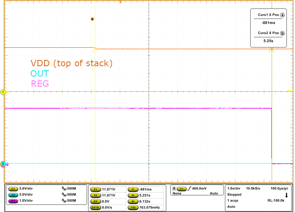
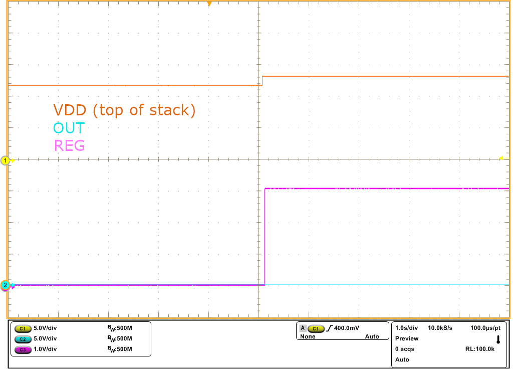
The scope plots below show the response of the device transitioning among the different states. Figure 8-4 shows the device detecting an overvoltage event and asserting the OUT pin to blow an external fuse after the overvoltage delay period. Figure 8-5 displays the device recovering from the overvoltage event when all cell voltages have fallen below the overvoltage threshold by the required hysteresis level, and the OUT pin deasserting. Figure 8-6 shows the device detecting an undervoltage condition and disabling the REG LDO output after the undervoltage delay period. Figure 8-7 then depicts the device recovering from the undervoltage condition and re-enabling the REG LDO when all cell voltages have risen above the undervoltage threshold by the required hysteresis level.
 Figure 8-4 Overvoltage Protection Triggering
 Figure 8-5 Overvoltage Protection Recovery
 Figure 8-6 Undervoltage Detection to Disable the Regulator
 Figure 8-7 Undervoltage Recovery to Re-enable the Regulator