SLUSF82A January   2024  – July 2024 LMG3100R017

PRODUCTION DATA  

  1.   1
  2. Features
  3. Applications
  4. Description
  5. Pin Configuration and Functions
  6. Specifications
    1. 5.1 Absolute Maximum Ratings
    2. 5.2 ESD Ratings
    3. 5.3 Recommended Operating Conditions
    4. 5.4 Thermal Information
    5. 5.5 Electrical Characteristics
    6. 5.6 Typical Characteristics
  7. Parameter Measurement Information
    1. 6.1 Propagation Delay and Mismatch Measurement
  8. Detailed Description
    1. 7.1 Overview
    2. 7.2 Functional Block Diagram
    3. 7.3 Feature Description
      1. 7.3.1 Control Inputs
      2. 7.3.2 Start-up and UVLO
      3. 7.3.3 Bootstrap Supply Voltage Clamping
      4. 7.3.4 Level Shift
    4. 7.4 Device Functional Modes
  9. Application and Implementation
    1. 8.1 Application Information
    2. 8.2 Typical Application
      1. 8.2.1 Design Requirements
      2. 8.2.2 Detailed Design Procedure
        1. 8.2.2.1 VCC Bypass Capacitor
        2. 8.2.2.2 Bootstrap Capacitor
        3. 8.2.2.3 Slew Rate Control
        4. 8.2.2.4 Use With Analog Controllers
        5. 8.2.2.5 Power Dissipation
      3. 8.2.3 Application Curves
    3. 8.3 Power Supply Recommendations
    4. 8.4 Layout
      1. 8.4.1 Layout Guidelines
      2. 8.4.2 Layout Examples
  10. Device and Documentation Support
    1. 9.1 Documentation Support
      1. 9.1.1 Related Documentation
    2. 9.2 Receiving Notification of Documentation Updates
    3. 9.3 Support Resources
    4. 9.4 Trademarks
    5. 9.5 Electrostatic Discharge Caution
    6. 9.6 Glossary
  11. 10Revision History
  12. 11Mechanical, Packaging, and Orderable Information
    1. 11.1 Package Information

Application Curves

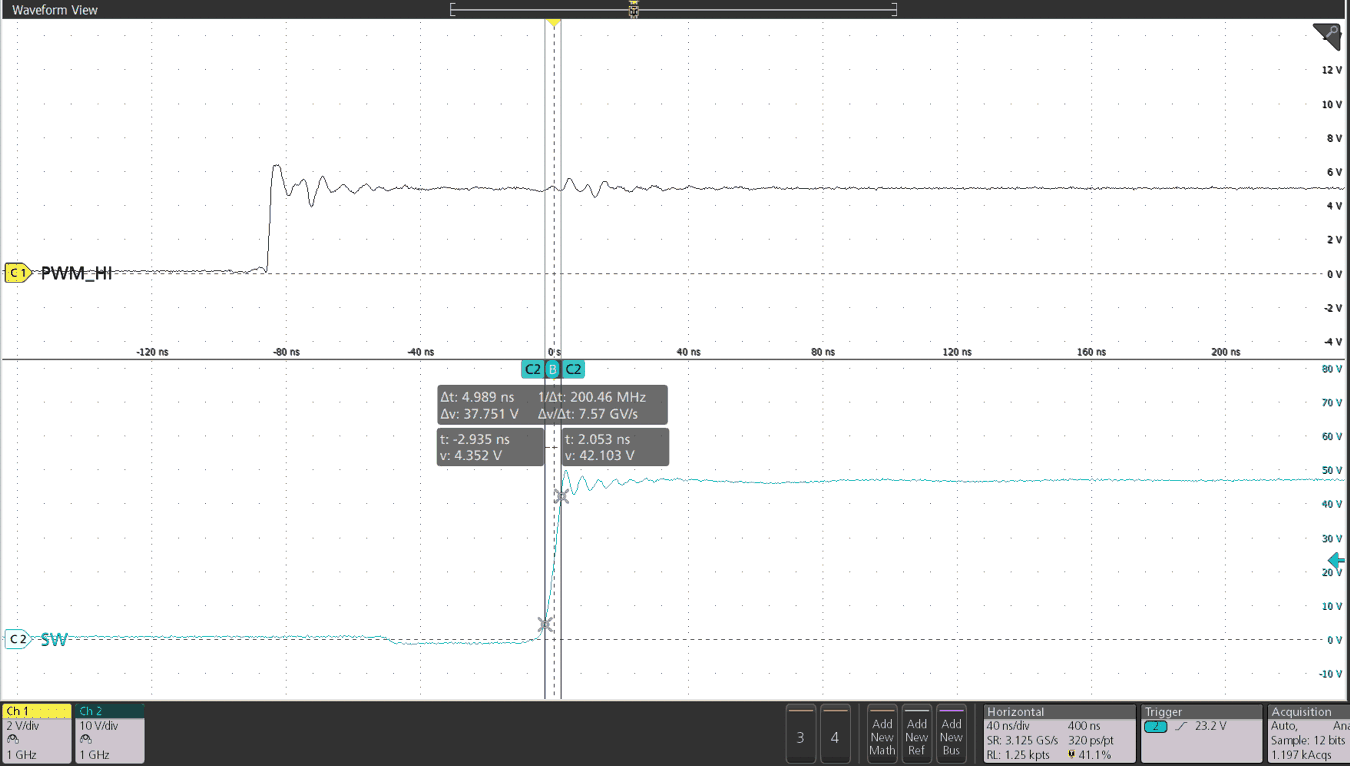
LMG3100R017 SW
                        Node Behavior Showing the Dead Time and Rise Time for RBST = 3 Ω
                        in a buck configuration
IOUT = 20 A VIN = 48 V VOUT = 24 V
Figure 8-4 SW Node Behavior Showing the Dead Time and Rise Time for RBST = 3 Ω in a buck configuration
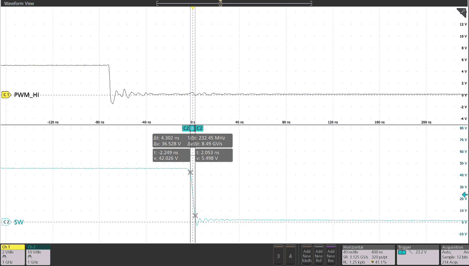
LMG3100R017 SW
                        node Falling Behavior in a buck configuration
IOUT = 20 A VIN = 48 V VOUT = 24 V
Figure 8-5 SW node Falling Behavior in a buck configuration