SLUSFA1A September 2024 – December 2024 TPS1214-Q1
PRODUCTION DATA
- 1
- 1 Features
- 2 Applications
- 3 Description
- 4 Device Comparison
- 5 Pin Configuration and Functions
- 6 Specifications
- 7 Parameter Measurement Information
-
8 Detailed Description
- 8.1 Overview
- 8.2 Functional Block Diagram
- 8.3
Feature Description
- 8.3.1 Charge Pump and Gate Driver Output (VS, GATE, BST, SRC)
- 8.3.2 Capacitive Load Driving
- 8.3.3 Overcurrent and Short-Circuit Protection
- 8.3.4 Analog Current Monitor Output (IMON)
- 8.3.5 NTC-Based Temperature Sensing (TMP) and Analog Monitor Output (ITMPO)
- 8.3.6 Fault Indication and Diagnosis (FLT, SCP_TEST)
- 8.3.7 Reverse Polarity Protection
- 8.3.8 Undervoltage Protection (UVLO)
- 8.4 Device Functional Modes
- 9 Application and Implementation
- 10Device and Documentation Support
- 11Revision History
- 12Mechanical, Packaging, and Orderable Information
9.2.3 Application Curves
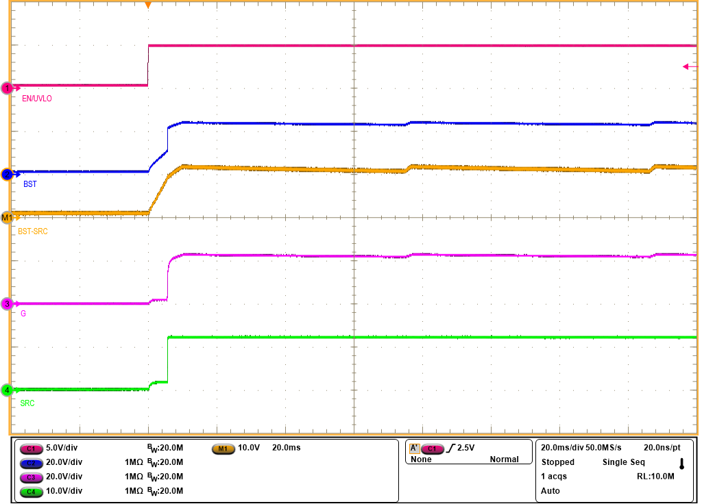 Figure 9-2 Start-Up Profile of Low
Power Path (LPM = Low, VIN = 12V, No Load,
CBST = 470nF)
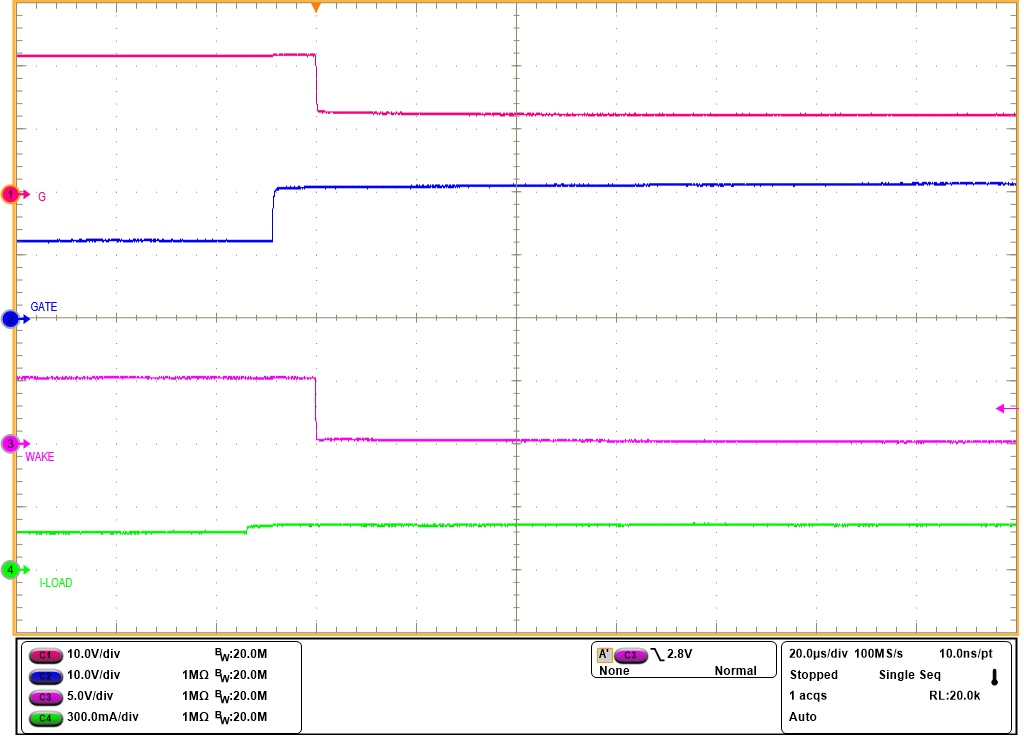 Figure 9-4 Zoom-In View of State
Transition From LPM to Active Mode (LPM = Low, VIN =
12V, EN/UVLO = High)
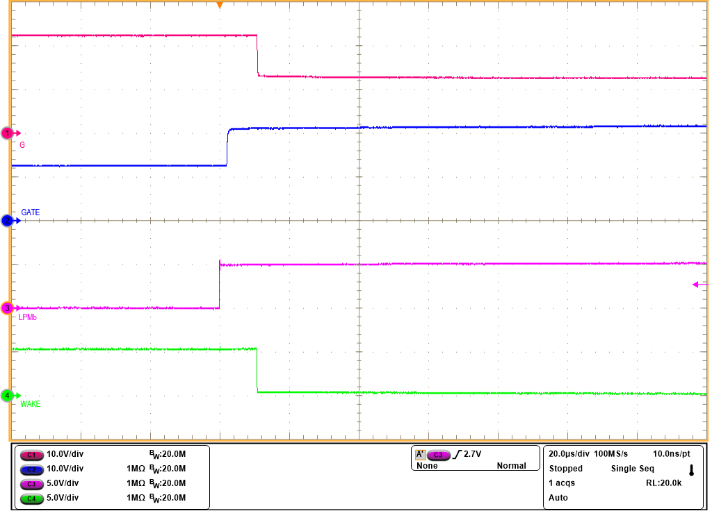 Figure 9-6 State Transition From LPM
to Active Mode (LPM = Low to High, VIN = 12V, No
Load)
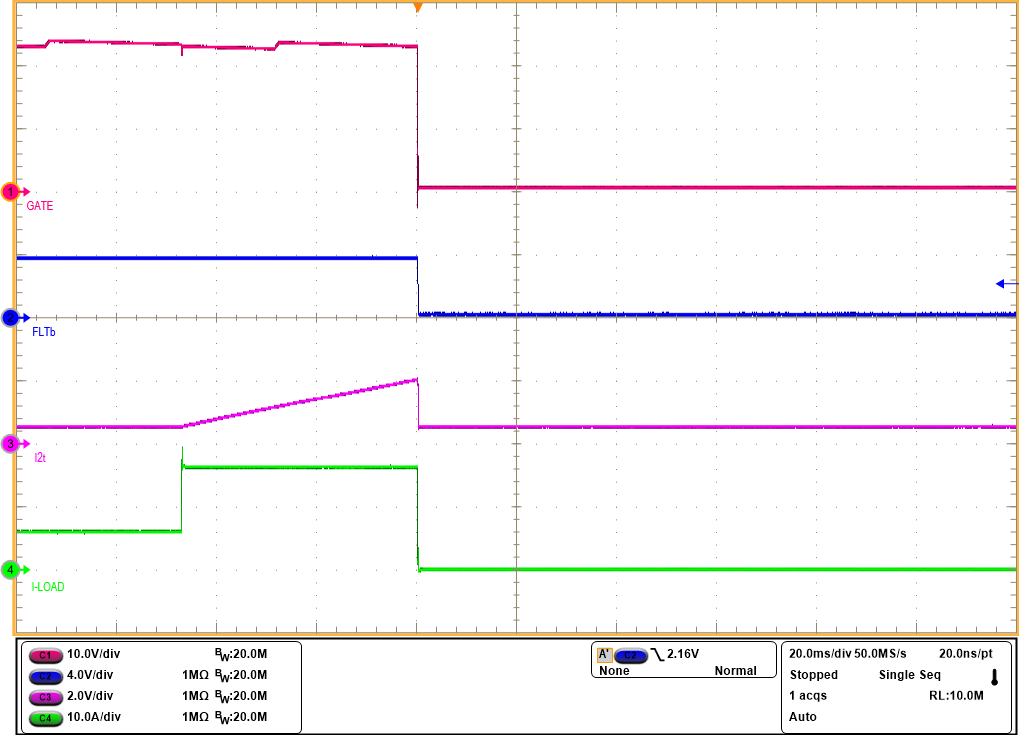 Figure 9-8 I2T based
Overcurrent Response of TPS1214-Q1 EVM for 6A to 16A Load Step
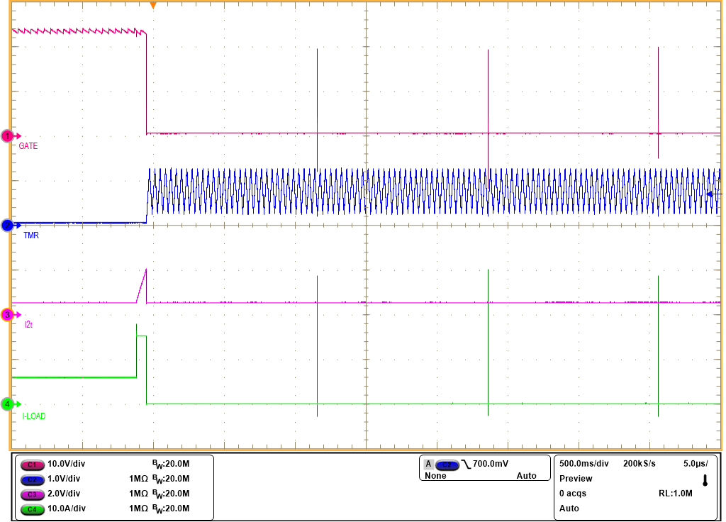 Figure 9-10 Auto-Retry Response of
TPS1214-Q1 for an I2T-Based Overcurrent Fault
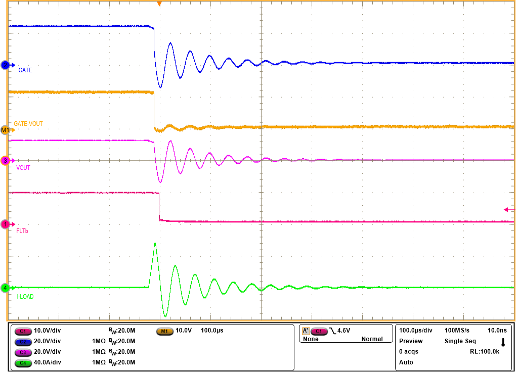 Figure 9-12 Output Short-Circuit Response of TPS1214-Q1
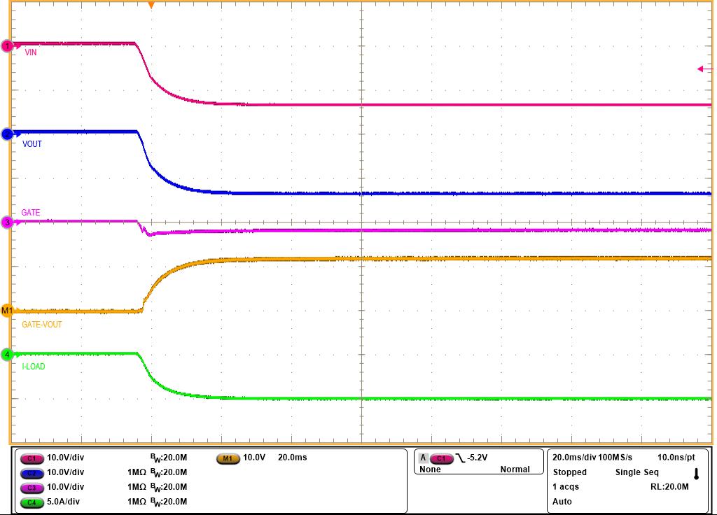 Figure 9-14 GATE Turn-ON During
Input Reverse Battery Fault for TPS12141-Q1 and TPS12143-Q1
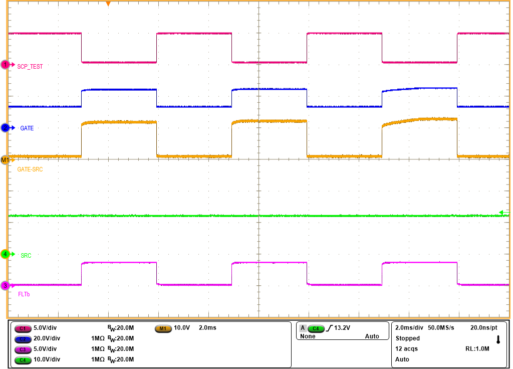 Figure 9-16 SCP_TEST Diagnosis in Active Mode (LPM =
High)
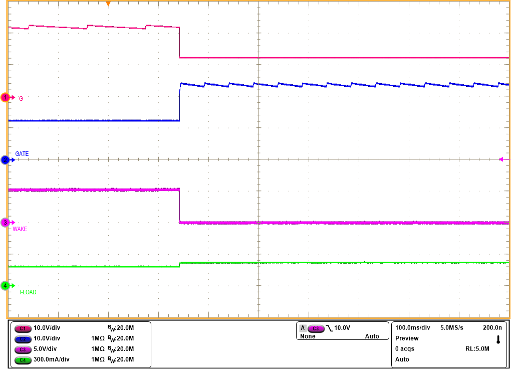 Figure 9-3 State Transition From LPM
to Active Mode (LPM = Low, VIN = 12V, EN/UVLO =
High)
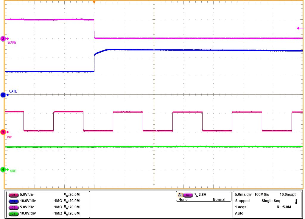 Figure 9-5 When LPM = Low in LOAD WAKEUP state, INP Has No
Control on GATE
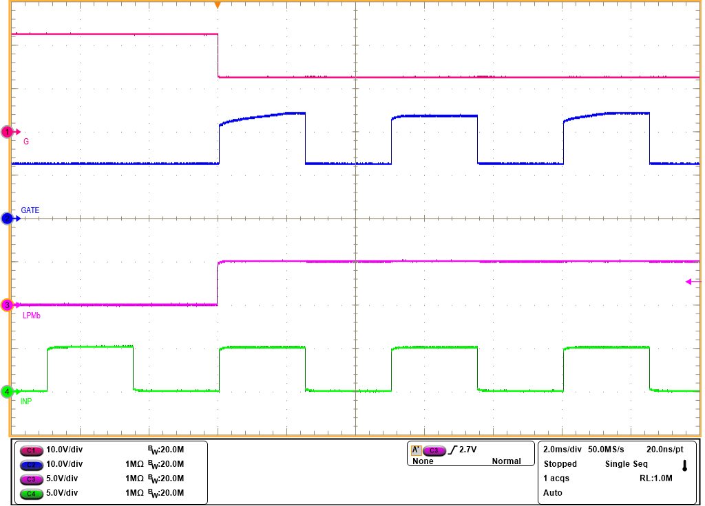 Figure 9-7 With
LPM = Low to High, INP Gained Control on GATE (VIN
= 12V, No Load)
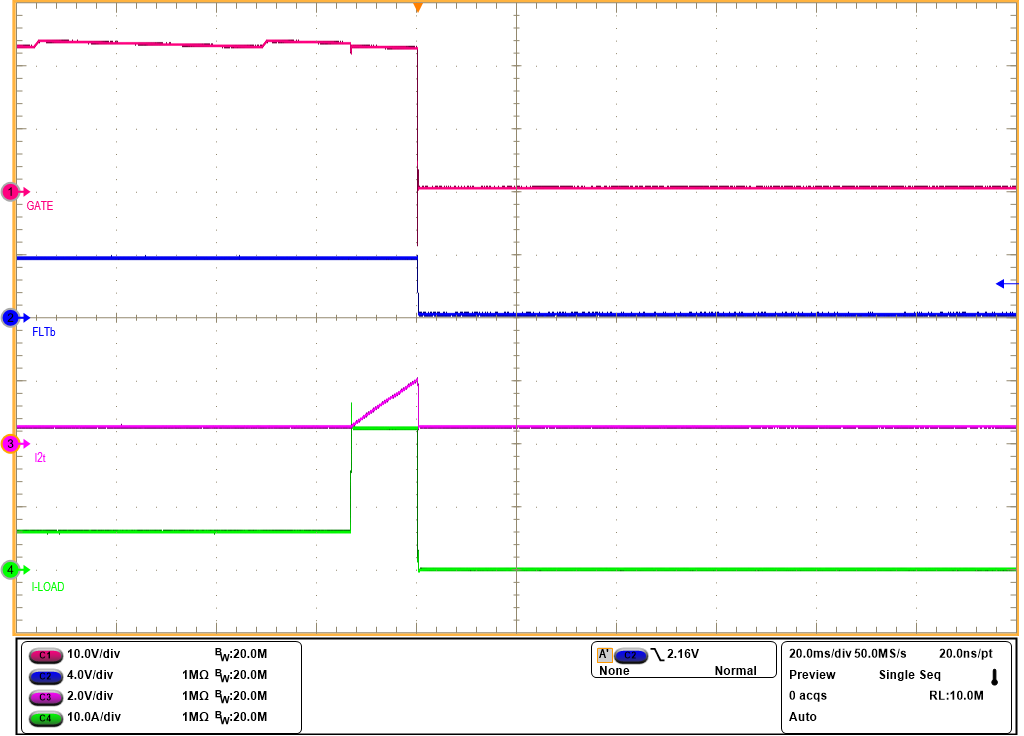 Figure 9-9 I2T based
Overcurrent Response of TPS1214-Q1 EVM for 6A to 23A Load Step
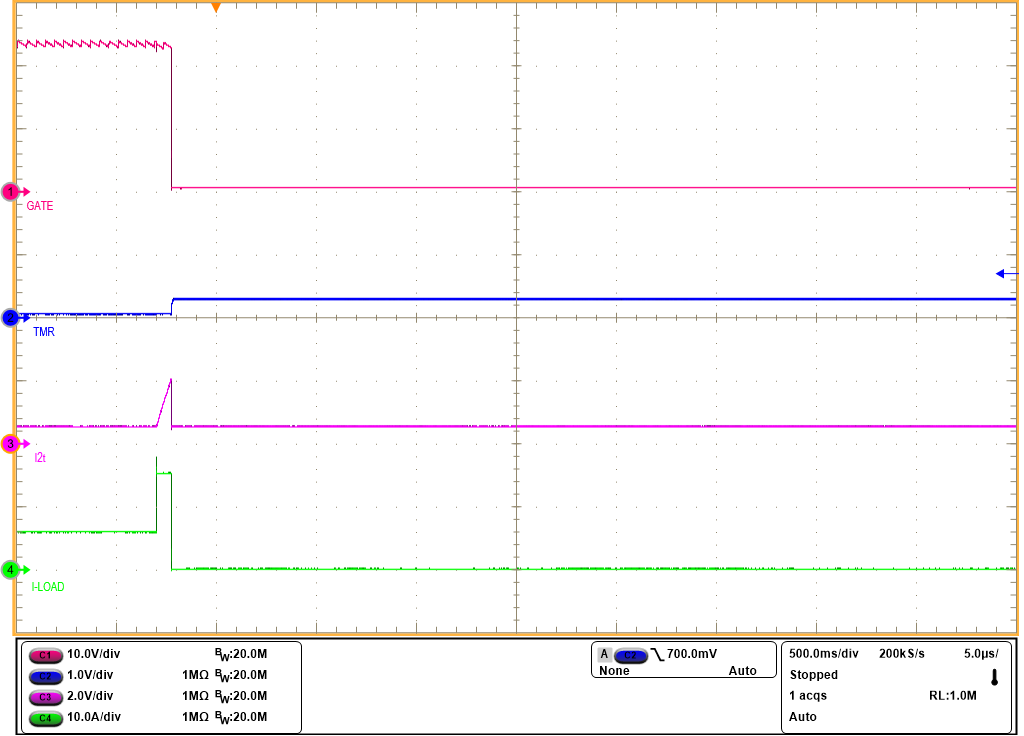 Figure 9-11 Latch-Off Response of
TPS1214-Q1 for an I2T-Based Overcurrent Fault
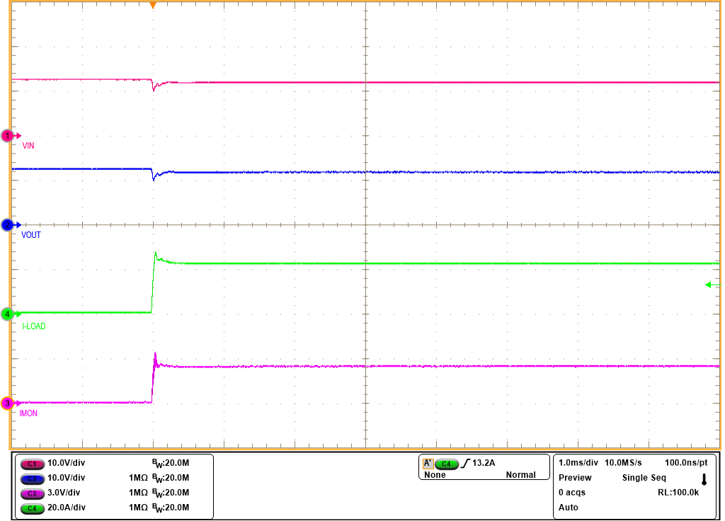 Figure 9-13 TPS1214-Q1 Current Monitoring Output (IMON) Transient Response
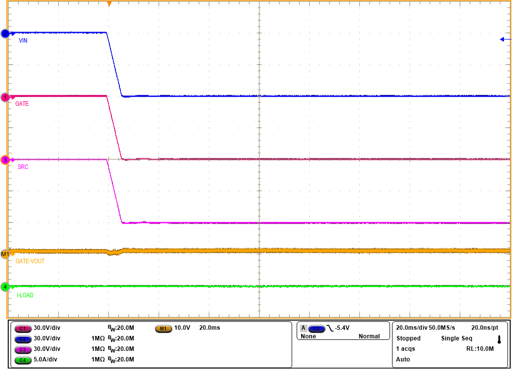 Figure 9-15 GATE Turn-OFF
During Input Reverse Battery Fault for TPS12140-Q1 and TPS12142-Q1
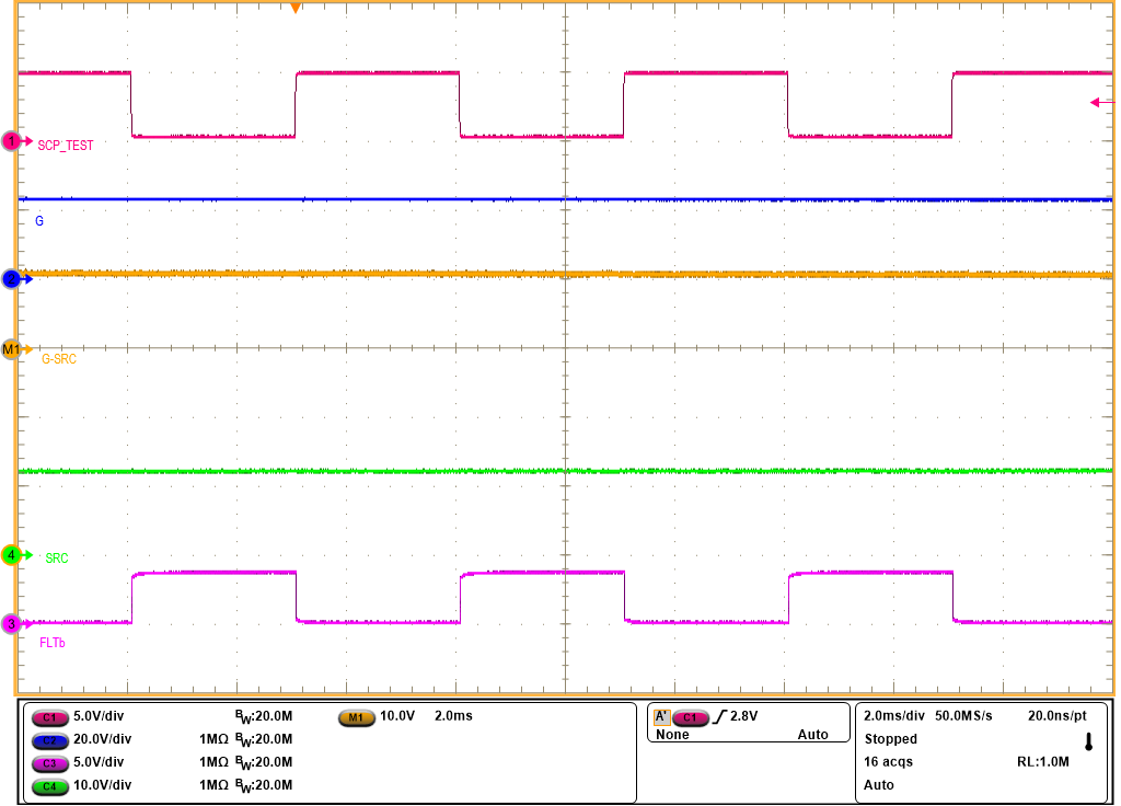 Figure 9-17 SCP_TEST Diagnosis in Low Power Mode (LPM =
Low)