SLUSFB7A September   2023  – June 2024 LMG3624

PRODUCTION DATA  

  1.   1
  2. Features
  3. Applications
  4. Description
  5. Pin Configuration and Functions
  6. Specifications
    1. 5.1 Absolute Maximum Ratings
    2. 5.2 ESD Ratings
    3. 5.3 Recommended Operating Conditions
    4. 5.4 Thermal Information
    5. 5.5 Electrical Characteristics
    6. 5.6 Switching Characteristics
    7. 5.7 Typical Characteristics
  7. Parameter Measurement Information
    1. 6.1 GaN Power FET Switching Parameters
  8. Detailed Description
    1. 7.1 Overview
    2. 7.2 Functional Block Diagram
    3. 7.3 Feature Description
      1. 7.3.1 GaN Power FET Switching Capability
      2. 7.3.2 Turn-On Slew-Rate Control
      3. 7.3.3 Current-Sense Emulation
      4. 7.3.4 Input Control Pins (EN, IN)
      5. 7.3.5 AUX Supply Pin
        1. 7.3.5.1 AUX Power-On Reset
        2. 7.3.5.2 AUX Under-Voltage Lockout (UVLO)
      6. 7.3.6 Overcurrent Protection
      7. 7.3.7 Overtemperature Protection
      8. 7.3.8 Fault Reporting
    4. 7.4 Device Functional Modes
  9. Application and Implementation
    1. 8.1 Application Information
    2. 8.2 Typical Application
      1. 8.2.1 Design Requirements
      2. 8.2.2 Detailed Design Procedure
        1. 8.2.2.1 Turn-On Slew-Rate Design
        2. 8.2.2.2 Current-Sense Design
      3. 8.2.3 Application Curves
    3. 8.3 Power Supply Recommendations
    4. 8.4 Layout
      1. 8.4.1 Layout Guidelines
        1. 8.4.1.1 Solder-Joint Stress Relief
        2. 8.4.1.2 Signal-Ground Connection
        3. 8.4.1.3 CS Pin Signal
      2. 8.4.2 Layout Example
  10. Device and Documentation Support
    1. 9.1 Documentation Support
      1. 9.1.1 Related Documentation
    2. 9.2 Receiving Notification of Documentation Updates
    3. 9.3 Support Resources
    4. 9.4 Trademarks
    5. 9.5 Electrostatic Discharge Caution
    6. 9.6 Glossary
  11. 10Revision History
  12. 11Mechanical, Packaging, and Orderable Information

Application Curves

The following waveforms show typical switching waveforms. The blue trace is the LMG2622 drain voltage (switch node voltage) and the red trace is the CS pin current-sense emulation voltage.
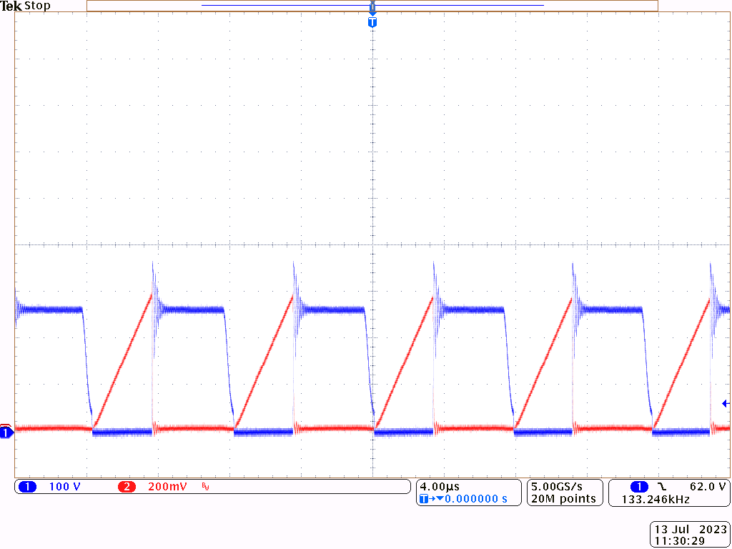

LMG3624 VIN = 115VAC
              VOUT = 20V IOUT = 3.25A

Figure 8-2 VIN = 115VAC VOUT = 20V IOUT = 3.25A
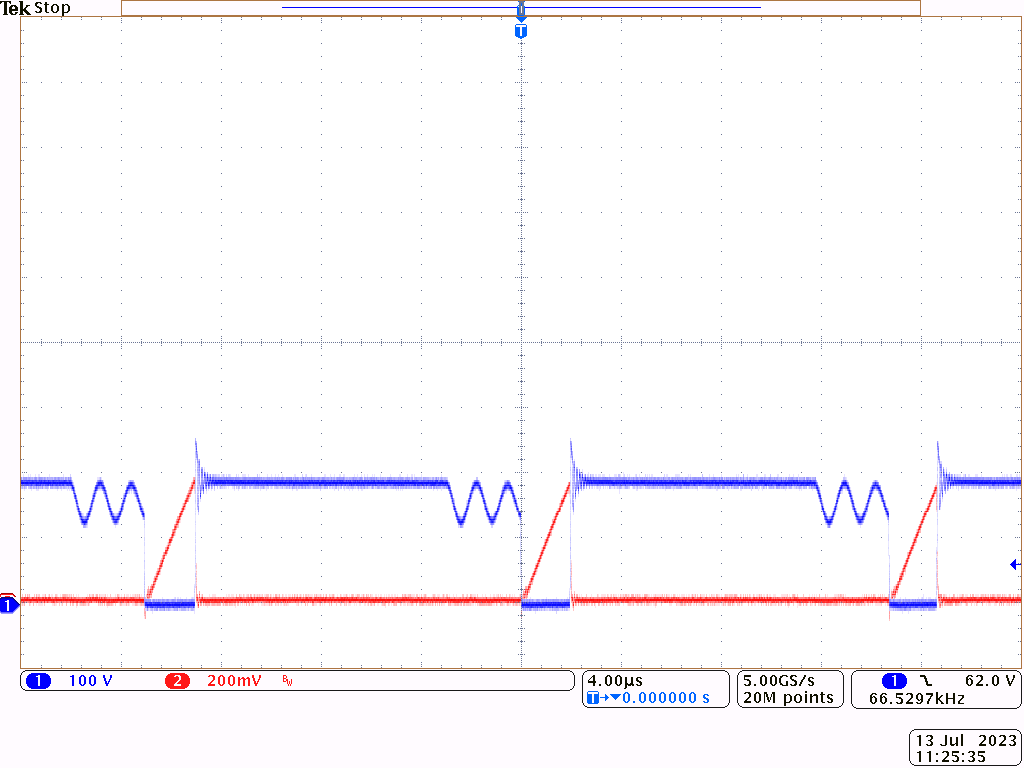
LMG3624 VIN = 115
              VACVOUT = 5V IOUT = 3A

Figure 8-4 VIN = 115 VACVOUT = 5V IOUT = 3A
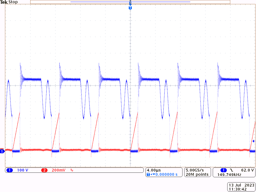
LMG3624 VIN = 230VAC
              VOUT = 20V IOUT = 3.25A

Figure 8-3 VIN = 230VAC VOUT = 20V IOUT = 3.25A
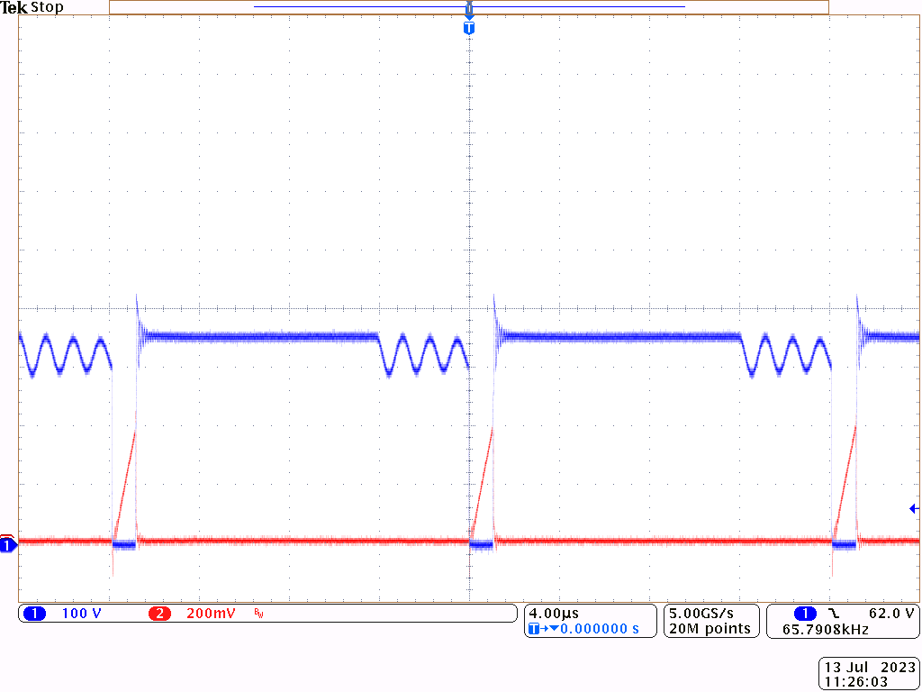
LMG3624 VIN = 230
              VACVOUT = 5V IOUT = 3A

Figure 8-5 VIN = 230 VACVOUT = 5V IOUT = 3A