SLUSFL6A June   2024  – November 2024 TPSM82866C

PRODMIX  

  1.   1
  2. Features
  3. Applications
  4. Description
  5. Device Options
  6. Pin Configuration and Functions
  7. Specifications
    1. 6.1 Absolute Maximum Ratings
    2. 6.2 ESD Ratings
    3. 6.3 Recommended Operating Conditions
    4. 6.4 Thermal Information
    5. 6.5 Electrical Characteristics
    6. 6.6 I2C Interface Timing Characteristics
    7. 6.7 Typical Characteristics
  8. Detailed Description
    1. 7.1 Overview
    2. 7.2 Functional Block Diagram
    3. 7.3 Feature Description
      1. 7.3.1 Power Save Mode
      2. 7.3.2 Forced PWM Mode
      3. 7.3.3 Optimized Transient Performance from PWM to PSM Operation
      4. 7.3.4 Low Dropout Operation (100% Duty Cycle)
      5. 7.3.5 Enable and Soft-Start Ramp
      6. 7.3.6 Switch Current Limit and HICCUP Short-Circuit Protection
      7. 7.3.7 Undervoltage Lockout
      8. 7.3.8 Thermal Warning and Shutdown
    4. 7.4 Device Functional Modes
      1. 7.4.1 Enable and Disable (EN)
      2. 7.4.2 Output Discharge
      3. 7.4.3 Start-Up Output Voltage and I2C Target Address Selection (VSET)
      4. 7.4.4 Select Output Voltage Registers (VID)
    5. 7.5 Programming
      1. 7.5.1 Serial Interface Description
      2. 7.5.2 Standard-Mode, Fast-Mode, and Fast-Mode Plus Protocol
      3. 7.5.3 HS-Mode Protocol
      4. 7.5.4 I2C Update Sequence
      5. 7.5.5 I2C Register Reset
  9. Register Map
    1. 8.1 Target Address Byte
    2. 8.2 Register Address Byte
    3. 8.3 VOUT Register 1
    4. 8.4 VOUT Register 2
    5. 8.5 CONTROL Register
    6. 8.6 STATUS Register
  10. Application and Implementation
    1. 9.1 Application Information
    2. 9.2 Typical Application
      1. 9.2.1 Design Requirements
      2. 9.2.2 Detailed Design Procedure
        1. 9.2.2.1 Input and Output Capacitor Selection
      3. 9.2.3 Application Curves
    3. 9.3 Power Supply Recommendations
    4. 9.4 Layout
      1. 9.4.1 Layout Guidelines
      2. 9.4.2 Layout Example
        1. 9.4.2.1 Thermal Considerations
  11. 10Device and Documentation Support
    1. 10.1 Device Support
      1. 10.1.1 Third-Party Products Disclaimer
    2. 10.2 Documentation Support
      1. 10.2.1 Related Documentation
    3. 10.3 Receiving Notification of Documentation Updates
    4. 10.4 Support Resources
    5. 10.5 Trademarks
    6. 10.6 Electrostatic Discharge Caution
    7. 10.7 Glossary
  12. 11Revision History
  13. 12Mechanical, Packaging, and Orderable Information

Application Curves

VIN = 5.0V, VOUT = 1.2V, TA = 25°C, BOM = Table 9-2, unless otherwise noted. Solid lines show the FPWM mode and dashed lines show PSM.

TPSM82866C Efficiency VIN = 5.0V and TA = 25°C
TPSM82866CAxPSM and FPWM
Figure 9-2 Efficiency VIN = 5.0V and TA = 25°C
TPSM82866C Efficiency VIN = 3.3V and TA = 25°C
TPSM82866CAxPSM and FPWM
Figure 9-4 Efficiency VIN = 3.3V and TA = 25°C
TPSM82866C Efficiency VIN = 2.8V and TA = 25°C
TPSM82866CAxPSM and FPWM
Figure 9-6 Efficiency VIN = 2.8V and TA = 25°C
TPSM82866C Load Regulation VIN = 5.0V and PSM
TA = 25°C
Figure 9-8 Load Regulation VIN = 5.0V and PSM
TPSM82866C Load Regulation VIN = 3.3V and PSM
TA = 25°C
Figure 9-10 Load Regulation VIN = 3.3V and PSM
TPSM82866C Load Regulation VIN = 2.8V and PSM
TA = 25°C
Figure 9-12 Load Regulation VIN = 2.8V and PSM
TPSM82866C Switching Frequency VIN = 5.0V
FPWMTA = 25°C
Figure 9-14 Switching Frequency VIN = 5.0V
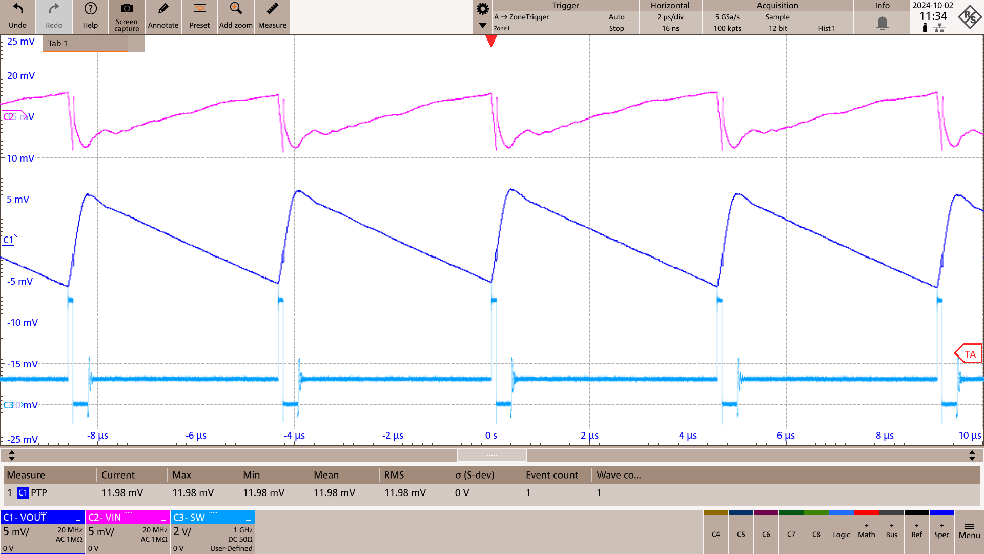
TPSM82866C FPWM Operation IOUT = 3A
VIN = 5.0VVOUT = 1.2V

COUT = 3 × 22uF

Figure 9-16 FPWM Operation IOUT = 3A
TPSM82866C FPWM Operation IOUT = 3A
VIN = 3.3VVOUT = 1.2V

COUT = 3 × 22uF

Figure 9-18 FPWM Operation IOUT = 3A
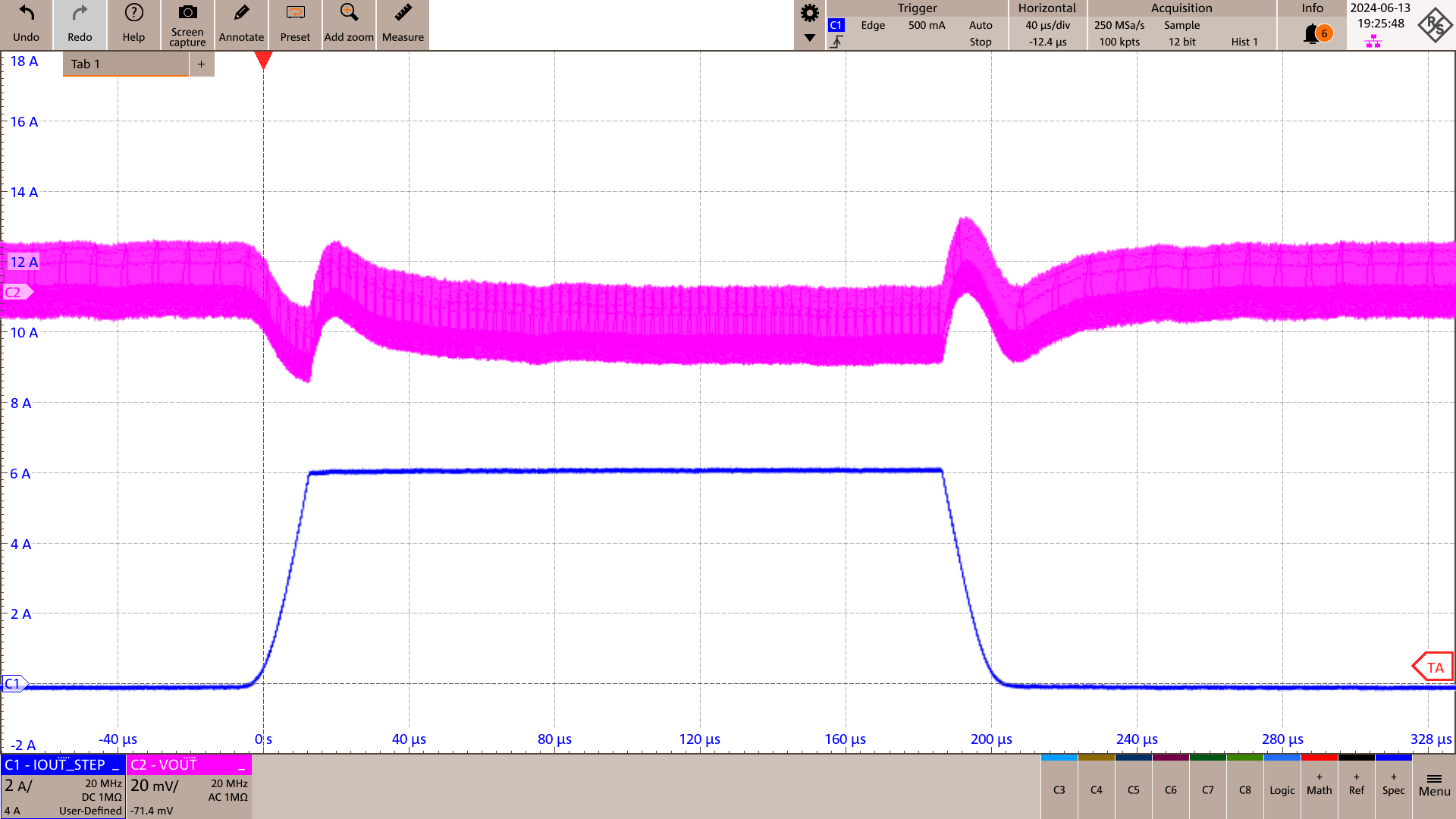
TPSM82866C Load Transient FPWM IOUT = 0A → 6A
VIN = 5.0VVOUT = 1.2VCOUT = 2 × 22uF
Figure 9-20 Load Transient FPWM IOUT = 0A → 6A
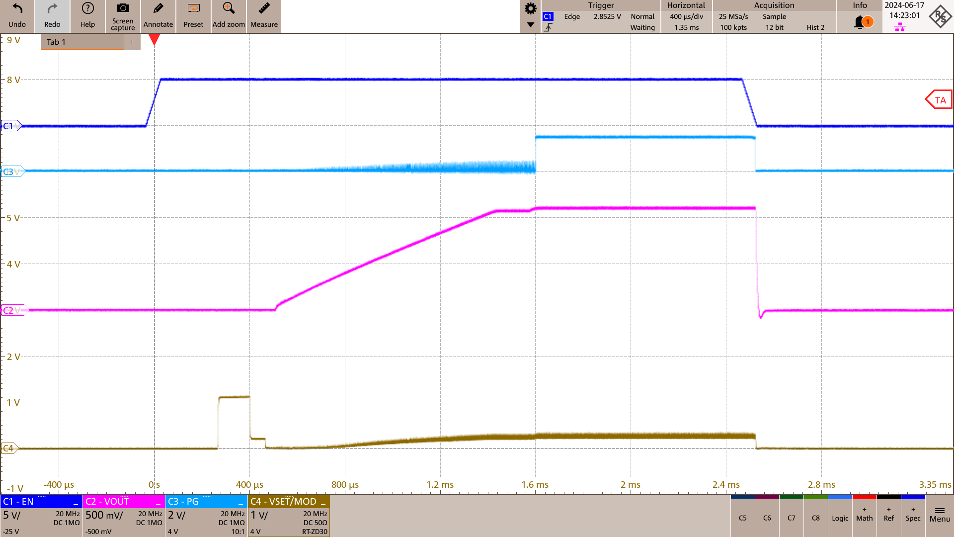
TPSM82866C Start-Up into Full Load
RVSET = 56.2kΩIOUT = 6.0A
Figure 9-22 Start-Up into Full Load
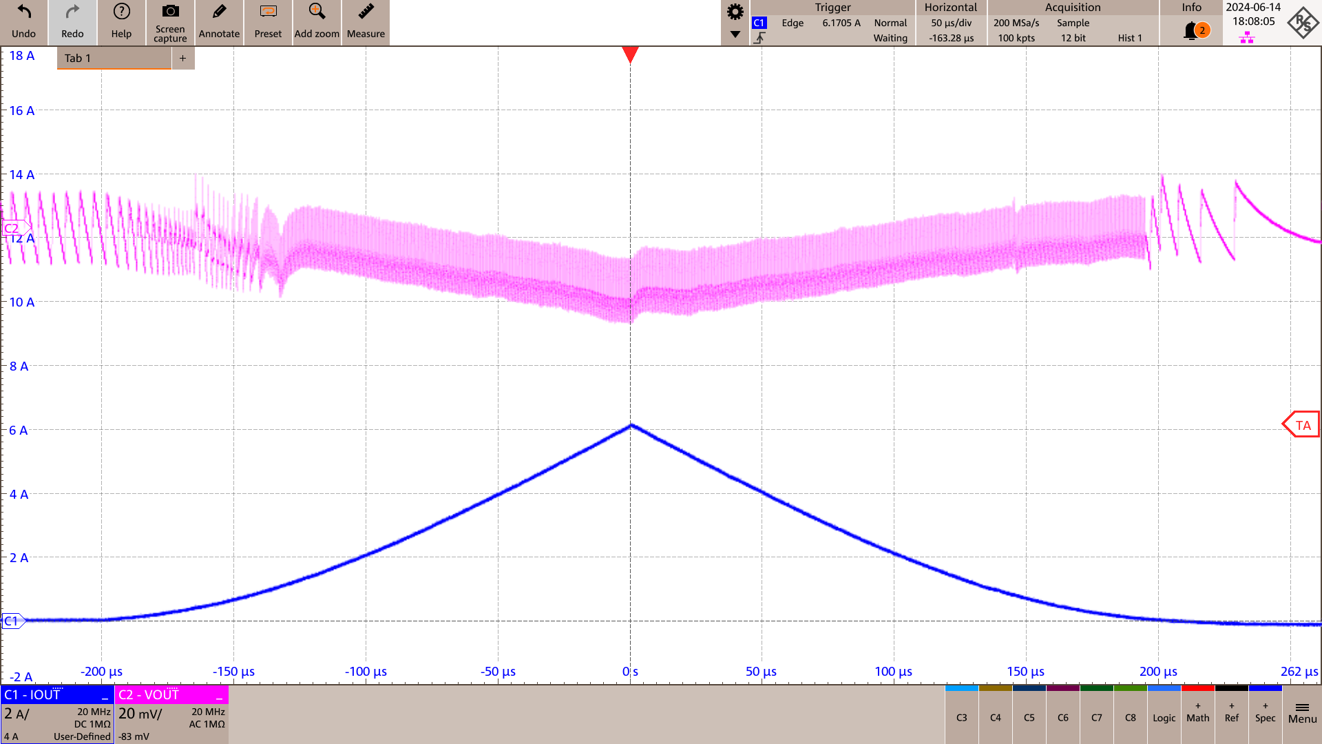
TPSM82866C Load Sweep IOUT = 20mA → 6A
VIN = 5.0VVOUT = 1.2VCOUT = 2 × 22uF
Figure 9-24 Load Sweep IOUT = 20mA → 6A
TPSM82866C Safe Operating Area VIN = 5.0V TPSM82866CAx
RθJA = 29.9°C/WTJmax = 125°C
Figure 9-26 Safe Operating Area VIN = 5.0V TPSM82866CAx
TPSM82866C Efficiency VIN = 5.0V and TA = 85°C
TPSM82866CAxPSM and FPWM
Figure 9-3 Efficiency VIN = 5.0V and TA = 85°C
TPSM82866C Efficiency VIN = 3.3V and TA = 85°C
TPSM82866CAx

PSM and FPWM

Figure 9-5 Efficiency VIN = 3.3V and TA = 85°C
TPSM82866C Efficiency VIN = 2.8V and TA = 85°C
TPSM82866CAxPSM and FPWM
Figure 9-7 Efficiency VIN = 2.8V and TA = 85°C
TPSM82866C Load Regulation VIN = 5.0V and FPWM
TA = 25°C
Figure 9-9 Load Regulation VIN = 5.0V and FPWM
TPSM82866C Load Regulation VIN = 3.3V and FPWM
TA = 25°C
Figure 9-11 Load Regulation VIN = 3.3V and FPWM
TPSM82866C Load Regulation VIN = 2.8V and FPWM
TA = 25°C
Figure 9-13 Load Regulation VIN = 2.8V and FPWM
TPSM82866C Switching Frequency VIN = 3.3V
FPWMTA = 25°C
Figure 9-15 Switching Frequency VIN = 3.3V
TPSM82866C PSM Operation IOUT = 0.1A
VIN = 5.0VVOUT = 1.2VCOUT = 3 × 22uF
Figure 9-17 PSM Operation IOUT = 0.1A
TPSM82866C FPWM Operation IOUT = 0.1A
VIN = 3.3VVOUT = 1.2VCOUT = 3 × 22uF
Figure 9-19 FPWM Operation IOUT = 0.1A
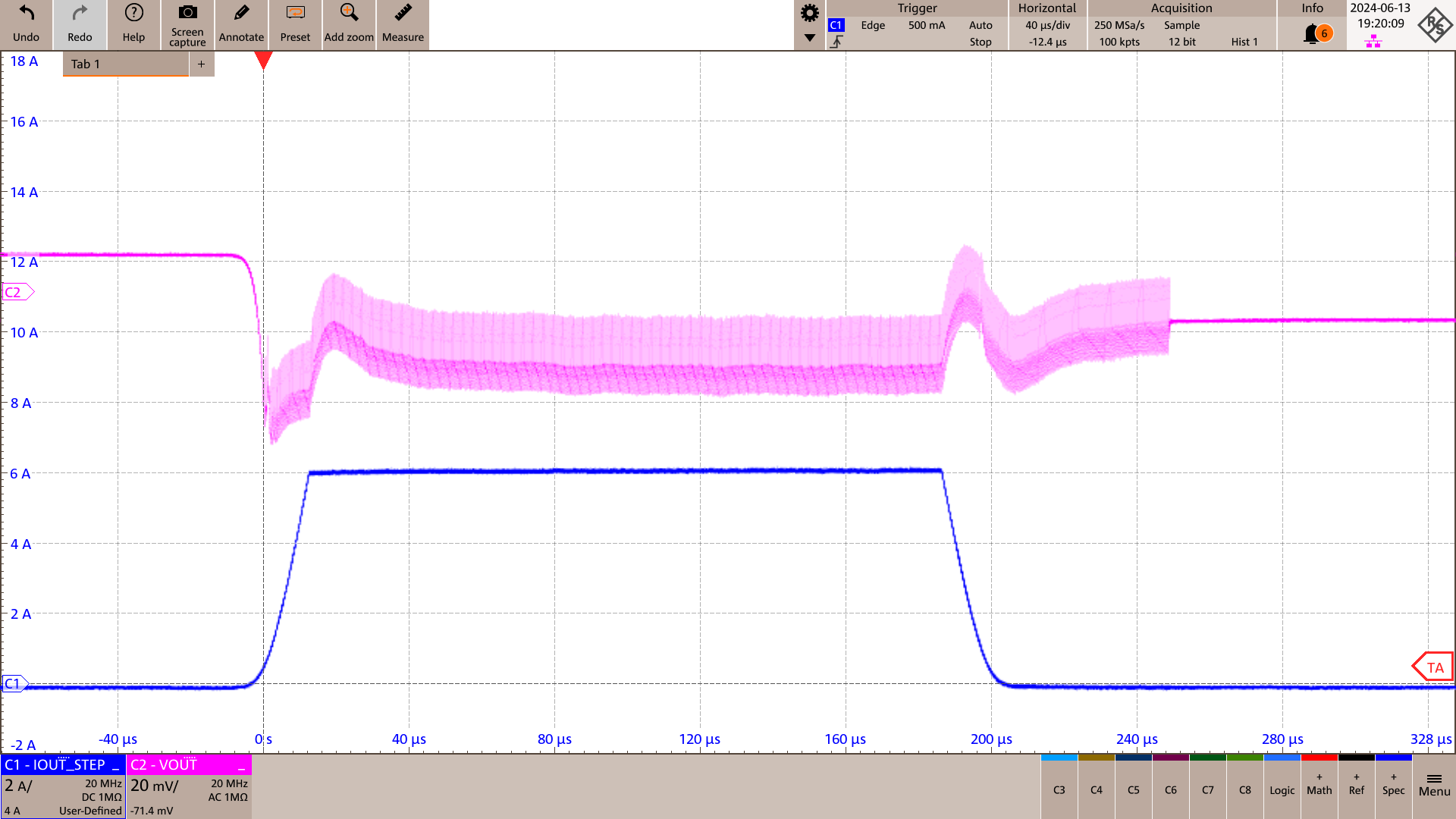
TPSM82866C Load Transient PSM IOUT = 0A → 6A
VIN = 5.0VVOUT = 1.2VCOUT = 2 × 22uF
Figure 9-21 Load Transient PSM IOUT = 0A → 6A
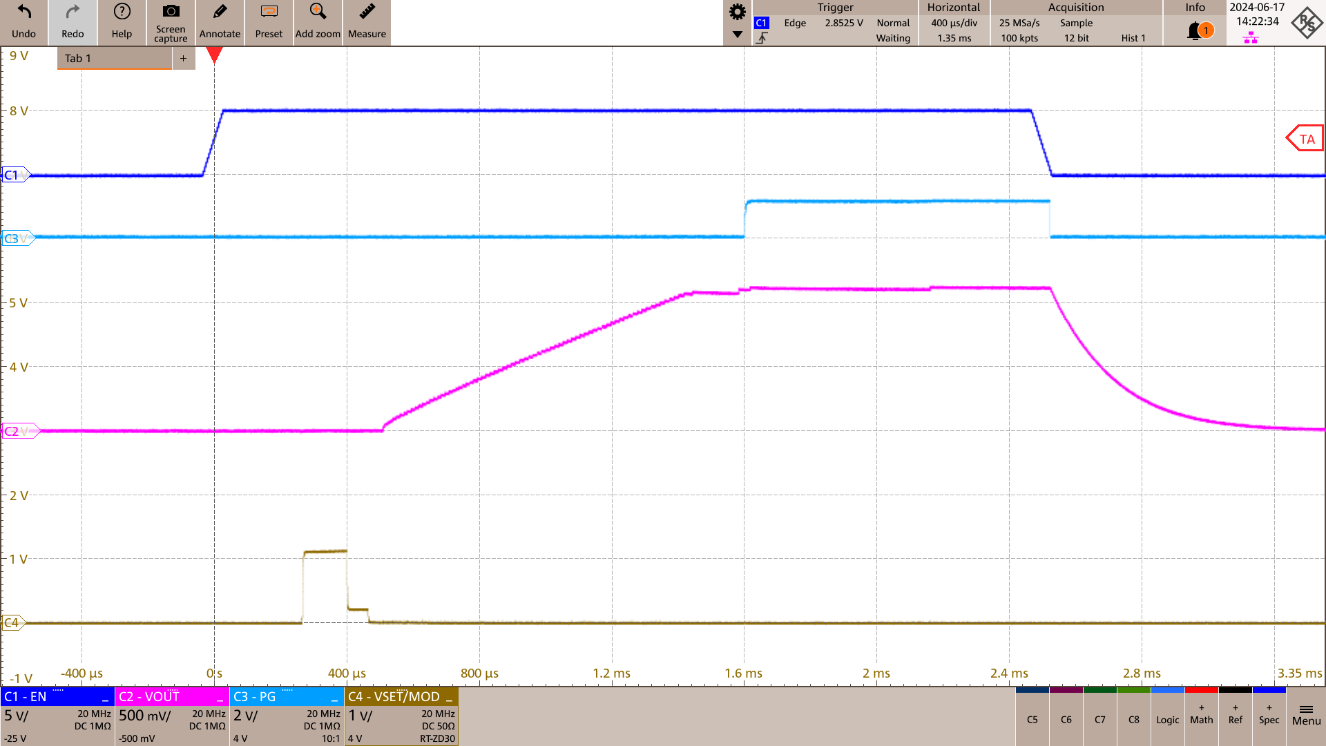
TPSM82866C Start-Up With No Load
RVSET = 56.2kΩIOUT = 0A
Figure 9-23 Start-Up With No Load
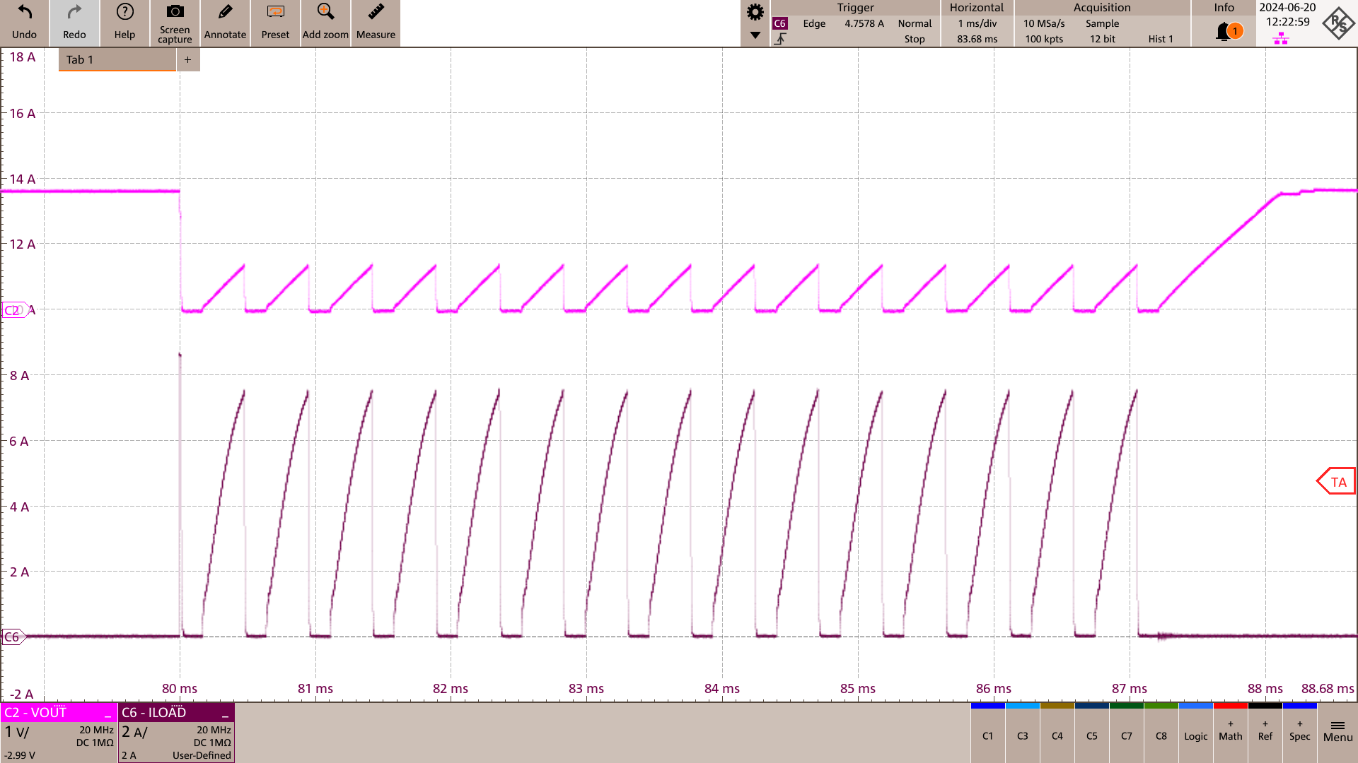
TPSM82866C HICCUP Short-Circuit Protection
RLOAD = 100mΩ (during overload)
Figure 9-25 HICCUP Short-Circuit Protection
TPSM82866C Safe Operating Area VIN = 3.3V TPSM82866CAx
RθJA = 29.9°C/WTJmax = 125°C
Figure 9-27 Safe Operating Area VIN = 3.3V TPSM82866CAx