SLUSFO3
November 2024
LMR51603
PRODUCTION DATA
1
1
Features
2
Applications
3
Description
4
Device Comparison Table
5
Pin Configuration and Functions
6
Specifications
6.1
Absolute Maximum Ratings
6.2
ESD Ratings
6.3
Recommended Operating Conditions
6.4
Thermal Information
6.5
Electrical Characteristics
6.6
Typical Characteristics
7
Detailed Description
7.1
Overview
7.2
Functional Block Diagram
7.3
Feature Description
7.3.1
Fixed Frequency Peak Current Mode Control
7.3.2
Adjustable Output Voltage
7.3.3
Enable
7.3.4
Minimum ON Time, Minimum OFF Time, and Frequency Foldback
7.3.5
Bootstrap Voltage
7.3.6
Overcurrent and Short-Circuit Protection
7.3.7
Soft Start
7.3.8
Thermal Shutdown
7.4
Device Functional Modes
7.4.1
Shutdown Mode
7.4.2
Active Mode
7.4.3
CCM Mode
7.4.4
Light Load Operation (PFM Version)
7.4.5
Light-Load Operation (FPWM Version)
8
Application and Implementation
8.1
Application Information
8.2
Typical Application
8.2.1
Design Requirements
8.2.2
Detailed Design Procedure
8.2.2.1
Custom Design With WEBENCH® Tools
8.2.2.2
Output Voltage Setpoint
8.2.2.3
Switching Frequency
8.2.2.4
Inductor Selection
8.2.2.5
Output Capacitor Selection
8.2.2.6
Input Capacitor Selection
8.2.2.7
Bootstrap Capacitor
8.2.2.8
Undervoltage Lockout Setpoint
8.2.2.9
Replacing Non-Sync Buck Converter
8.2.3
Application Curves
8.3
Power Supply Recommendations
8.4
Layout
8.4.1
Layout Guidelines
8.4.1.1
Compact Layout for EMI Reduction
8.4.1.2
Feedback Resistors
8.4.2
Layout Example
9
Device and Documentation Support
9.1
Device Support
9.1.1
Third-Party Products Disclaimer
9.1.2
Development Support
9.1.2.1
Custom Design With WEBENCH® Tools
9.2
Documentation Support
9.2.1
Related Documentation
9.3
Receiving Notification of Documentation Updates
9.4
Support Resources
9.5
Trademarks
9.6
Electrostatic Discharge Caution
9.7
Glossary
10
Revision History
11
Mechanical, Packaging, and Orderable Information
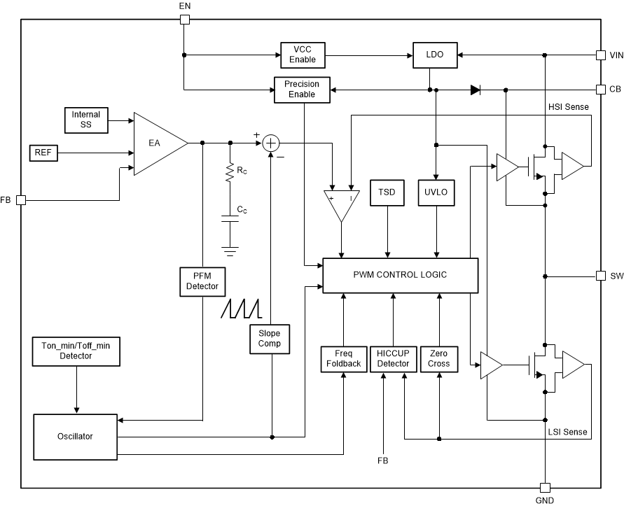
7.2
Functional Block Diagram