SLUU182A January   2004  – March 2022 TPS5124


  1.   Trademarks
  2. 1Introduction
  3. 2Features
  4. 3Schematic
  5. 4Design Procedure
    1. 4.1 Frequency Setting
    2. 4.2 Inductance Value
    3. 4.3 Output Capacitors
    4. 4.4 Input Capacitors
      1. 4.4.1 Case One: D1, D2 < 0.5
      2. 4.4.2 Case Two: D2 < 0.5 < D1
    5. 4.5 Compensation Design
    6. 4.6 Current Limiting
    7. 4.7 Timer Latch
      1. 4.7.1 Undervoltage Protection
      2. 4.7.2 Short Circuit Protection
      3. 4.7.3 Overvoltage Protection
      4. 4.7.4 Disabling the Protection Function
        1. 4.7.4.1 Disabling the Overcurrent Protection
        2. 4.7.4.2 Disabling the Overvoltage Protection or Undervoltage Protection
  6. 5Test Results
    1. 5.1 Efficiency Curves
    2. 5.2 Typical Operating Waveform
    3. 5.3 Start-Up Waveform
    4. 5.4 Output Ripple Voltage and Load Transient
  7. 6Layout Guidelines
    1. 6.1 Low-Side MOSFET
    2. 6.2 Connections
    3. 6.3 Bypass Capacitor
    4. 6.4 Bootstrap Capacitor
    5. 6.5 Output Voltage
  8. 7PCB Layout
  9. 8List of Materials
  10. 9Revision History

Start-Up Waveform

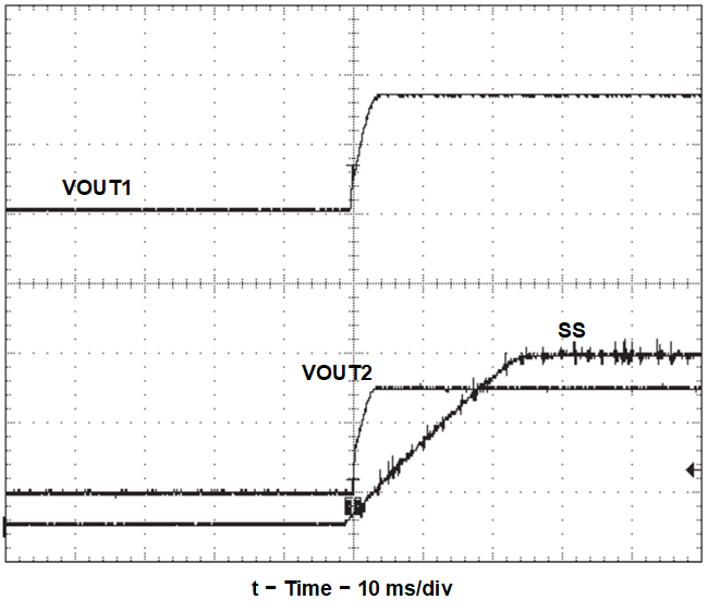
Figure 5-5 shows the start-up waveform taken at VIN = 12 V, IOUT1 = 15 A, and IOUT2 = 10 A. The rising time is 2.85 ms for VOUT1 and 2.12 ms for VOUT2.
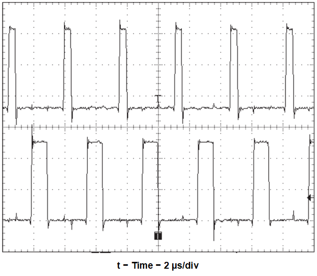
GUID-20220302-SS0I-5JWM-HDFS-VDC4DPT2M8SL-low.pngFigure 5-4 Switch Node Waveform
GUID-20220302-SS0I-CDHQ-22VN-CCRSVVKVCL9V-low.pngFigure 5-5 Start-Up Waveform