SLUUBG8C November   2018  – October 2021 UCC20520 , UCC21320-Q1 , UCC21520 , UCC21520-Q1 , UCC21521 , UCC21530


  1.   Trademarks
  2. Introduction
  3. Description
  4. Features
    1. 3.1 I/O Description
    2. 3.2 Jumpers (Shunt) Setting
  5. Electrical Specifications
  6. Test Summary
    1. 5.1 Definitions
    2. 5.2 Equipment
      1. 5.2.1 Power Supplies
      2. 5.2.2 Function Generators
    3. 5.3 Equipment Setup
      1. 5.3.1 DC Power Supply Settings
      2. 5.3.2 Digital Multi-Meter Settings
      3. 5.3.3 Two-Channel Function Generator Settings
      4. 5.3.4 Oscilloscope Setting
      5. 5.3.5 Jumper (Shunt) Settings
      6. 5.3.6 Bench Setup Diagram
  7. Power-Up and Power-Down Procedure
    1. 6.1 Power Up
    2. 6.2 Power Down
  8. Test Waveforms (CL=0pF) With Different DT Configurations
    1. 7.1 DT Connected to VCCI (J-DT Option B in Table 1-1 )
    2. 7.2 DT Pin Floating or Left Open (J-DT Option A in Table 1-1 )
    3. 7.3 DT Pin Connected to RDT (J-DT Option C in Table 1-1 )
  9. Schematic
  10. Layout Diagrams
  11. 10List of Materials
  12. 11Revision History

Layout Diagrams

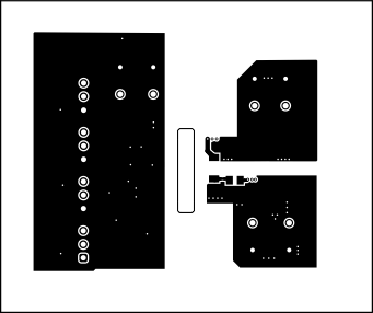
The PCB layout information for UCC21520EVM is shown in Figure 9-1, Figure 9-2, Figure 9-3, and Figure 9-4. The layouts are the same for UCC20520EVM, UCC21521CEVM, and UCC21530EVM except for the labels that designate the EVM part number with the device under test.
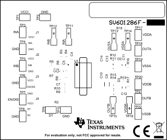
GUID-20210429-CA0I-WKPQ-J9VV-QF0P4SFFTSFG-low.gifFigure 9-1 Top Overlay
GUID-20210429-CA0I-SSXT-RD3K-TXQMB3WCB25X-low.gifFigure 9-3 Bottom Layer
GUID-20210505-CA0I-TM0F-NQCP-FLLVJVRDZNXQ-low.gifFigure 9-2 Top Layer
GUID-20210429-CA0I-5DH8-HFL0-HBFKFKR27M4R-low.gifFigure 9-4 Bottom Overlay