SLUUC03A February 2019 – December 2022 TPS566235
4.2 Board Layout
Figure 4-2 through Figure 4-6 illustrates the TPS566235EVM-036 board layout. The top layer contains the main power traces for VIN, VOUT, and SW, there is a large area filled with ground. The internal layer-1 and layer-2 are ground plane. The bottom layer is another ground plane. The ground traces of each layer are connected together with multiple VIAs. The top and bottom layers are 2-oz copper and internal layers are 1-oz copper.
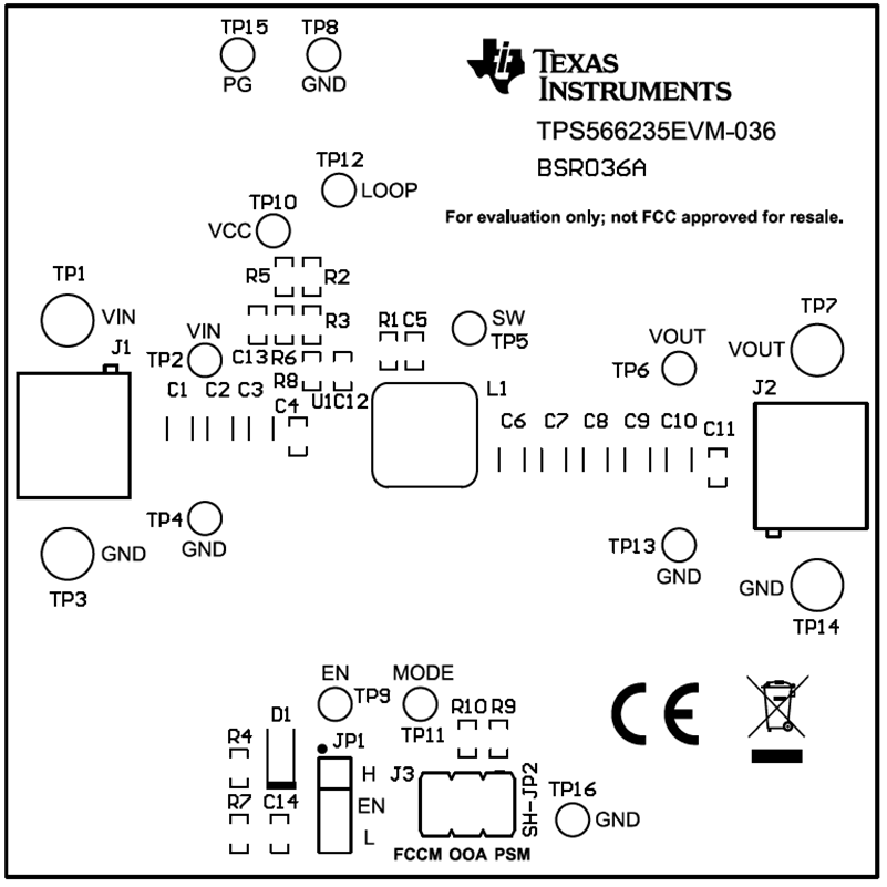 Figure 4-2 Component Placement (Top Layer)
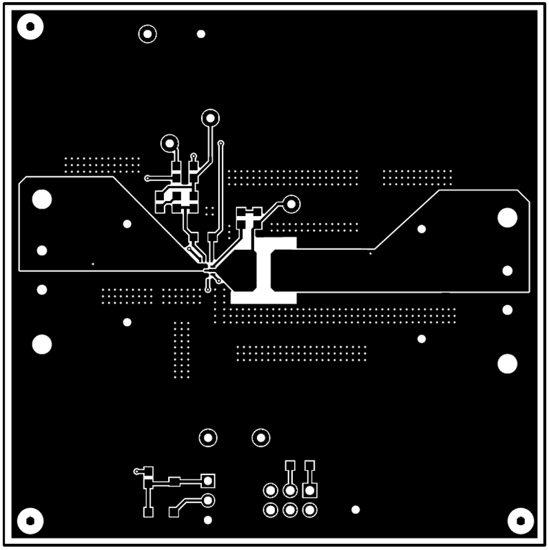 Figure 4-3 Board Layout (Top Layer)
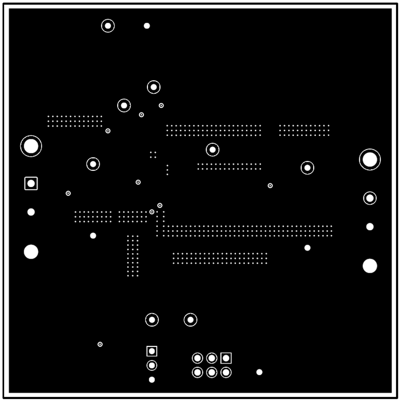 Figure 4-4 Board Layout (Second Layer)
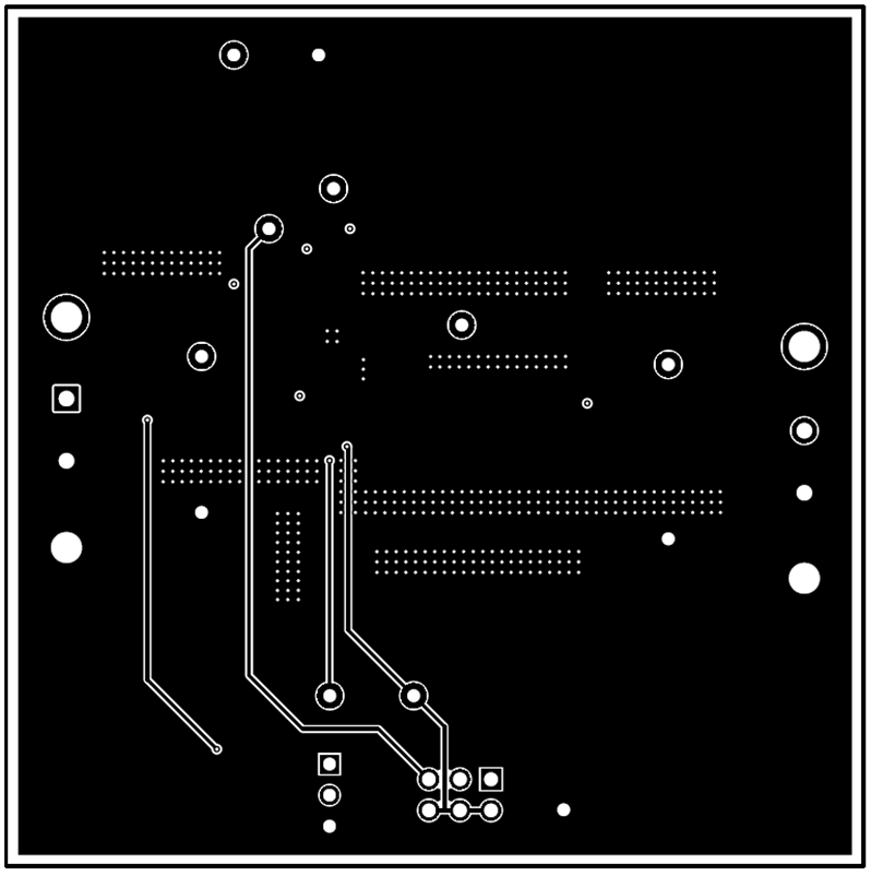 Figure 4-5 Board Layout (Third Layer)
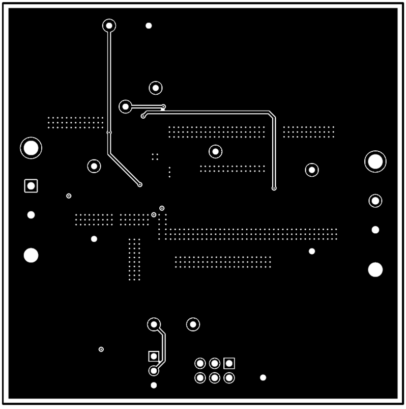 Figure 4-6 Board Layout (Bottom Layer)