SLUUC03A February   2019  – December 2022 TPS566235


  1.   TPS566235EVM-036 evaluation module
  2.   Trademarks
  3. 1Introduction
  4. 2Specification Summary
  5. 3Modifications
    1. 3.1 Output Voltage Setpoint
    2. 3.2 Mode Selection
  6. 4Schematic and Board layout
    1. 4.1 Schematic
    2. 4.2 Board Layout
  7. 5EVM Test Setup
    1. 5.1 Connectors and Jumpers Description and Placement
    2. 5.2 Start-up Procedure
  8. 6Test Waveforms
    1. 6.1 Power Up
    2. 6.2 Power Down
    3. 6.3 Output Voltage Ripple
    4. 6.4 Load Transient Response
    5. 6.5 Thermal
  9. 7List of Materials and Reference
    1. 7.1 List of Materials
    2. 7.2 Reference
  10. 8Revision History

Power Down

Figure 6-2 shows the power down waveform at 12-V input and 1.05-V output. Once the EN signal is low, VOUT starts to ramp down.
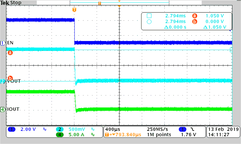
GUID-2AC65D5B-A54A-40A6-927E-781D9535BB43-low.gif Figure 6-2 Power Down with 6-A Loading Controlled by EN Pin