SLUUC03A February 2019 – December 2022 TPS566235
5.1 Connectors and Jumpers Description and Placement
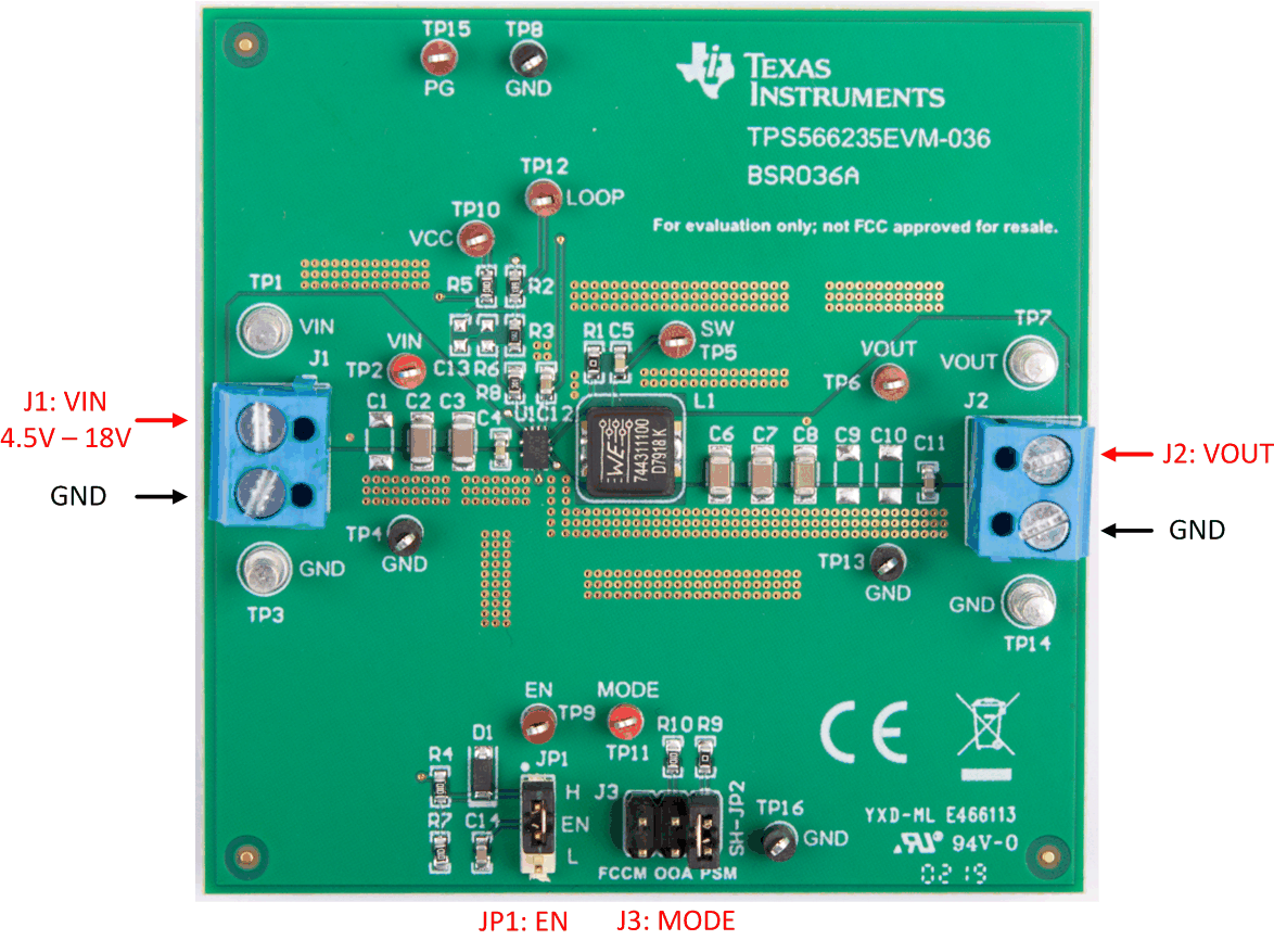
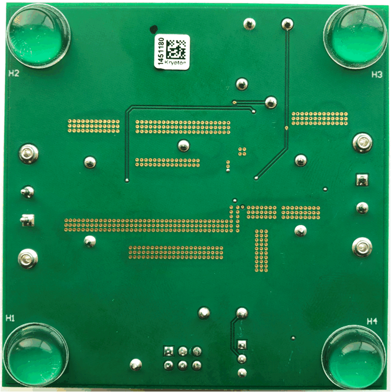
TPS566235EVM-036 is provided with input/output connectors and test points as listed in Table 5-1. And Figure 5-1 and Figure 5-2 shows connectors and jumpers placement on TPS566235EVM-036 board.
A power supply capable of supplying greater than 5 A must be connected to J1 through a pair of 20-AWG wires. The load must be connected to J2 through a pair of 20-AWG wires. The maximum load current capability is 6 A. Wire lengths must be minimized to reduce losses in the wires. Test point TP2 provides a place to monitor the VIN input voltages with TP4 providing a convenient ground reference. TP6 is used to monitor the output voltage with TP13 as the ground reference.
 Figure 5-1 Connectors and Jumpers
Placement (Top View)
 Figure 5-2 Connectors and Jumpers
Placement (Bottom View)
Figure 5-2 Connectors and Jumpers
Placement (Bottom View)| DESIGNATOR | FUNCTION | DESCRIPTION |
|---|---|---|
| J1 | VIN connector | Connect input power supply |
| J2 | VOUT connector | Connect output load |
| J3 | MODE selection | Refer to Table 3-1 for operation mode selection |
| JP1 | Enable/disable control | Middle pin is IC's EN pin. Floating EN or shunting to GND will disable IC; Shunting EN to the other side will enable IC |
| TP1, TP2 | VIN test point | Test input voltage |
| TP3, TP4, TP8, TP13, TP14, TP16 |
GND test point | Ground reference |
| TP5 | SW test point | Test switching node |
| TP6, TP7 | VOUT test point | Test output voltage |
| TP9 | EN test point | Test enable signal |
| TP10 | VCC test point | Test VCC |
| TP11 | MODE test point | Test MODE |
| TP12 | Loop test point | Test point between voltage divider network and output, used for loop response measurement |
| TP15 | PG test point | Test power good signal |