SLUUC67A August 2020 – April 2021 TPS562202
4.1 Input/Output Connections
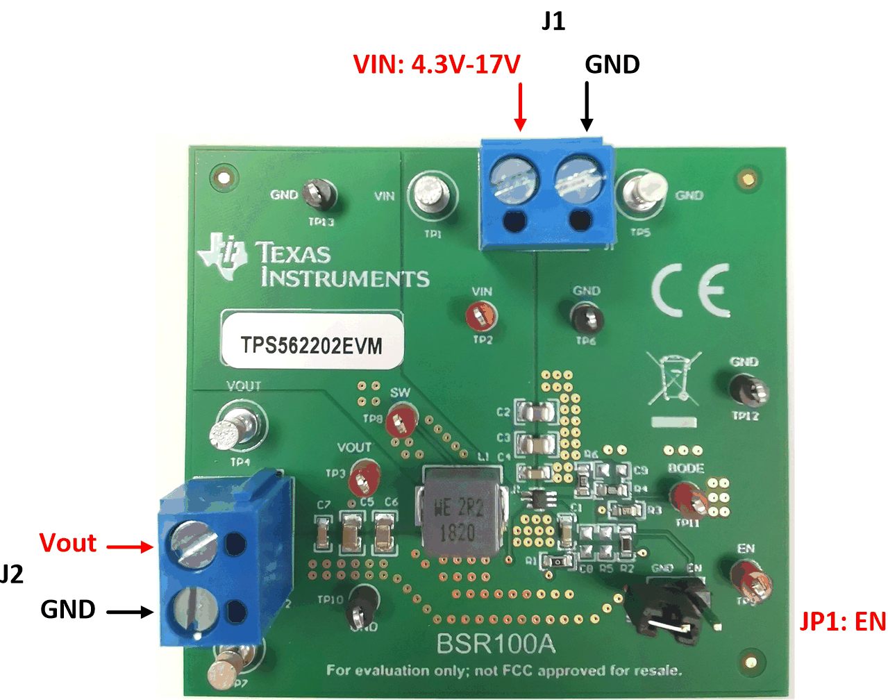
The TPS562202EVM is provided with input/output connectors and test points as shown in Table 4-1. Figure 4-1 shows connectors and jumpers placement on TPS562202EVM board.
A power supply capable of supplying 2 A must be connected to J1 through a pair of 20-AWG wires. The load must be connected to J2 through a pair of 20-AWG wires. The maximum load current capability is 2 A. Wire lengths must be minimized to reduce losses in the wires. Test point TP2 provides a place to monitor the VIN input voltages with TP6 providing a convenient ground reference. TP3 is used to monitor the output voltage with TP10 as the ground reference.
 Figure 4-1 TPS562202EVM
Connectors and Jumpers Placement
Figure 4-1 TPS562202EVM
Connectors and Jumpers Placement| REFERENCE DESIGNATOR | FUNCTION |
|---|---|
| J1 | VIN (see Table 1-1 for VIN range) |
| J2 | VOUT, 1.05 V at 2-A maximum |
| JP1 | EN control. Shunt EN to GND to disable |
| TP1 | VIN positive power point |
| TP2 | VIN positive monitor point |
| TP3 | VOUT positive monitor point |
| TP4 | VOUT positive power point |
| TP5, TP7 | GND power point |
| TP6, TP10, TP12,TP13 | GND monitor point |
| TP8 | Switch node test point |
| TP9 | EN test point |
| TP11 | Test point for loop response measurements |