SLUUC85B June   2020  – September 2020 TPS62860 , TPS62861


  1.   Trademarks
  2. 1Introduction
    1. 1.1 Background
    2. 1.2 Performance Specification
    3. 1.3 Modifications
      1. 1.3.1 IC U1 Operation
  3. 2Setup
    1. 2.1 Input and Output Connector Description
      1. 2.1.1 J1, Pin 1 and 2 – VIN
      2. 2.1.2 J1, Pin 3 and 4 – S+/S-
      3. 2.1.3 J1, Pin 5 and 6 – GND
      4. 2.1.4 J2, Pin 1 and 2 – VOUT
      5. 2.1.5 J2, Pin 3 and 4 – S+/S-
      6. 2.1.6 J2, Pin 5 and 6 – GND
      7. 2.1.7 J3 – I2C
      8. 2.1.8 JP1 – EN
      9. 2.1.9 JP2 – VSEL
    2. 2.2 Setup
  4. 3Board Layout
    1. 3.1 Layout
  5. 4Schematic and Bill of Materials
    1. 4.1 Schematic
    2. 4.2 Bill of Materials
  6. 5Software User Interface
    1. 5.1 Software Setup
    2. 5.2 Interface Hardware Setup
    3. 5.3 User Interface Operation
      1. 5.3.1 Home Screen
      2. 5.3.2 Settings Screen
      3. 5.3.3 Register Map Screen
  7.   Revision History

Layout

Figure 3-1 through Figure 3-5 show the component placement and PCB layout of the TPS62861xEVM.

GUID-20200917-CA0I-QT4T-ZCWS-XCGGLCBWFN8Q-low.svgFigure 3-1 TPS6286x0EVM PCB - Assembly Layer
GUID-20200917-CA0I-MXN5-N8K9-J3RPMJ8VFV0B-low.svgFigure 3-2 TPS6286x0EVM PCB - Top Layer
GUID-20200917-CA0I-DS1T-T1R6-LVWSTNJ4QXW6-low.svgFigure 3-3 TPS6286x0EVM PCB - Signal Layer 1 (Top View)
GUID-20200917-CA0I-52NT-TSHP-X0ZHMBW9P51V-low.svgFigure 3-4 TPS6286x0EVM PCB - Signal Layer 2 (Top View)
GUID-20200921-CA0I-6MRC-CLFB-X54D2PNN8KLN-low.svgFigure 3-5 TPS6286x0EVM PCB - Bottom Layer (Top View)
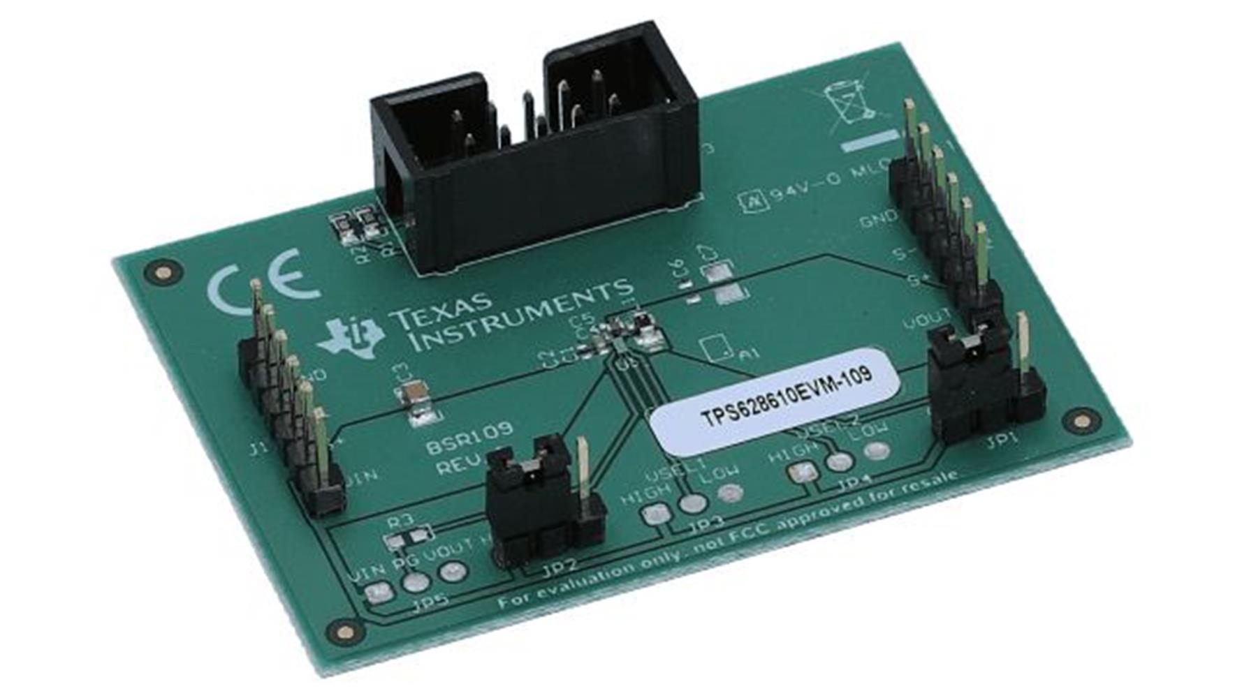
GUID-564CA5AB-1D92-4D44-8665-ED60E8CC713C-low.jpgFigure 3-6 TPS628610EVM Angled View
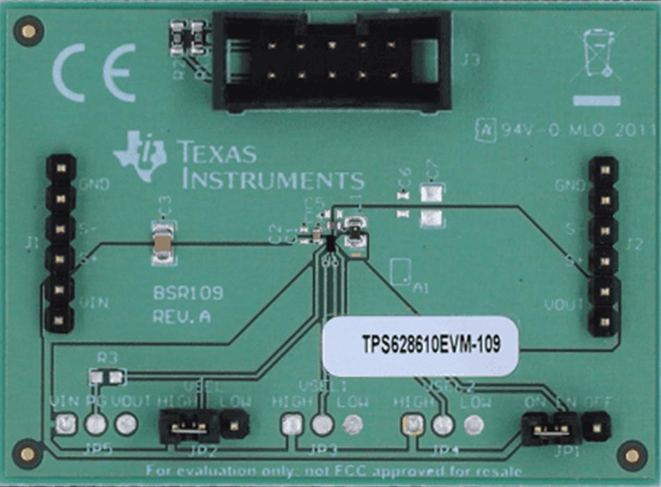
GUID-11FEA758-0610-4550-8655-92B7D1E9AD7F-low.jpgFigure 3-7 TPS628610EVM Overhead View