SLUUC85B June   2020  – September 2020 TPS62860 , TPS62861


  1.   Trademarks
  2. 1Introduction
    1. 1.1 Background
    2. 1.2 Performance Specification
    3. 1.3 Modifications
      1. 1.3.1 IC U1 Operation
  3. 2Setup
    1. 2.1 Input and Output Connector Description
      1. 2.1.1 J1, Pin 1 and 2 – VIN
      2. 2.1.2 J1, Pin 3 and 4 – S+/S-
      3. 2.1.3 J1, Pin 5 and 6 – GND
      4. 2.1.4 J2, Pin 1 and 2 – VOUT
      5. 2.1.5 J2, Pin 3 and 4 – S+/S-
      6. 2.1.6 J2, Pin 5 and 6 – GND
      7. 2.1.7 J3 – I2C
      8. 2.1.8 JP1 – EN
      9. 2.1.9 JP2 – VSEL
    2. 2.2 Setup
  4. 3Board Layout
    1. 3.1 Layout
  5. 4Schematic and Bill of Materials
    1. 4.1 Schematic
    2. 4.2 Bill of Materials
  6. 5Software User Interface
    1. 5.1 Software Setup
    2. 5.2 Interface Hardware Setup
    3. 5.3 User Interface Operation
      1. 5.3.1 Home Screen
      2. 5.3.2 Settings Screen
      3. 5.3.3 Register Map Screen
  7.   Revision History

Settings Screen

The Settings screen provides control over the VOUT and CONTROL Registers. The Status Register is available in this window as well. Real-time updates are possible if the Auto Read function is set to As fast as possible in the Register Map page.
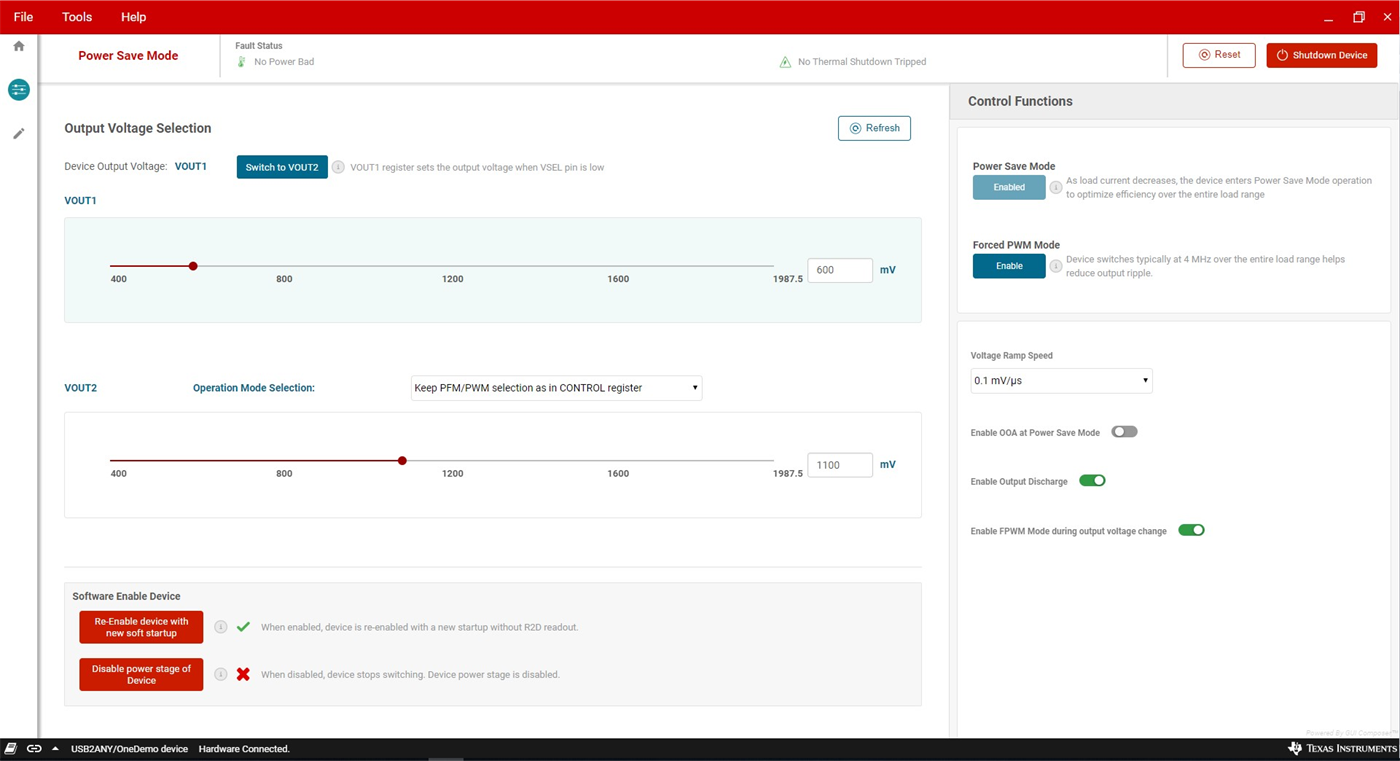
GUID-2280A1B6-1D3C-4434-8E68-27E8A99A713A-low.png Figure 5-3 GUI Settings Screen