SLUUCE4 June   2021


  1.   Trademarks
  2. 1Introduction
  3. 2Description
    1. 2.1 Features
    2. 2.2 I/O Description
  4. 3Electrical Specifications
  5. 4Test Summary
    1. 4.1 Definitions
    2. 4.2 Equipment
      1. 4.2.1 Power Supply
      2. 4.2.2 Function Generator
      3. 4.2.3 DMM
      4. 4.2.4 Oscilloscope
    3. 4.3 Equipment Setup
      1. 4.3.1 DC Power Supply Settings
      2. 4.3.2 Digital Multi-Meter Settings
      3. 4.3.3 Two-Channel Function Generator Settings
      4. 4.3.4 Oscilloscope Settings
      5. 4.3.5 Bench Setup Diagram
  6. 5Power Up and Power Down Procedure
    1. 5.1 Power Up
    2. 5.2 Power Down
  7. 6Typical Performance Waveforms (CL = 1800 pF)
    1. 6.1 Propagation Delays
  8. 7Schematic
  9. 8Layout Diagrams
  10. 9List of Materials

Layout Diagrams

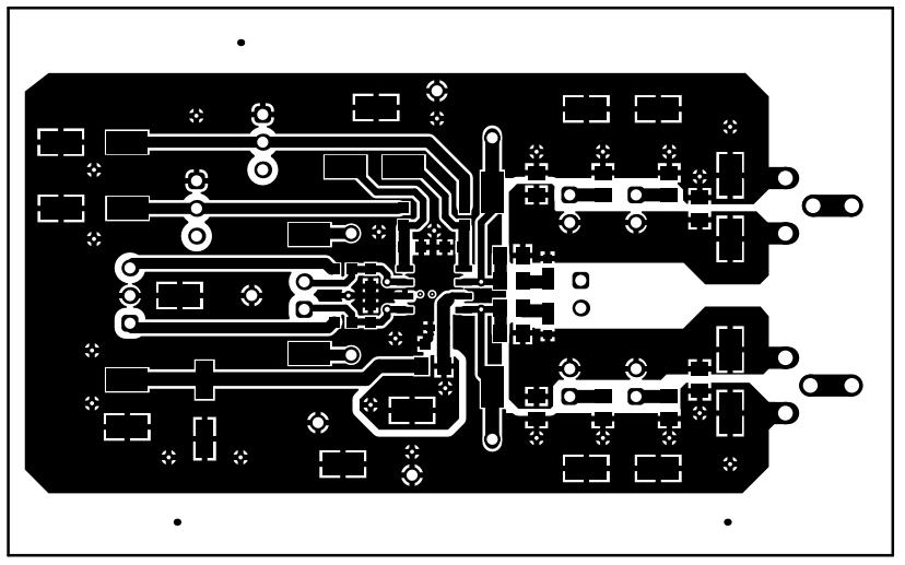
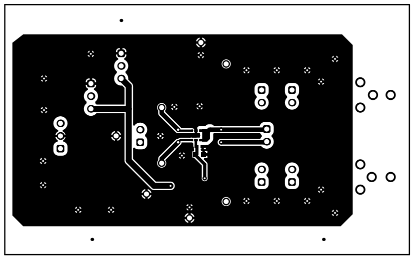
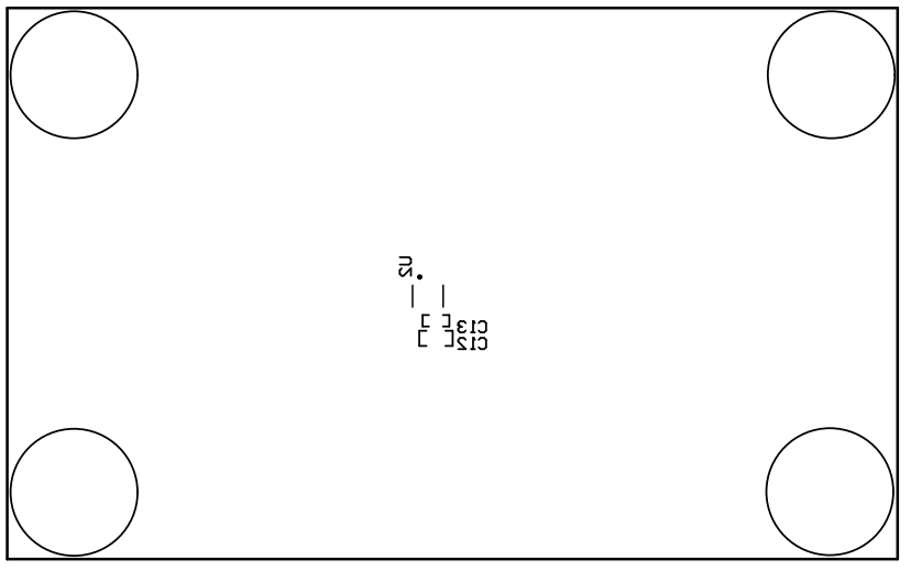
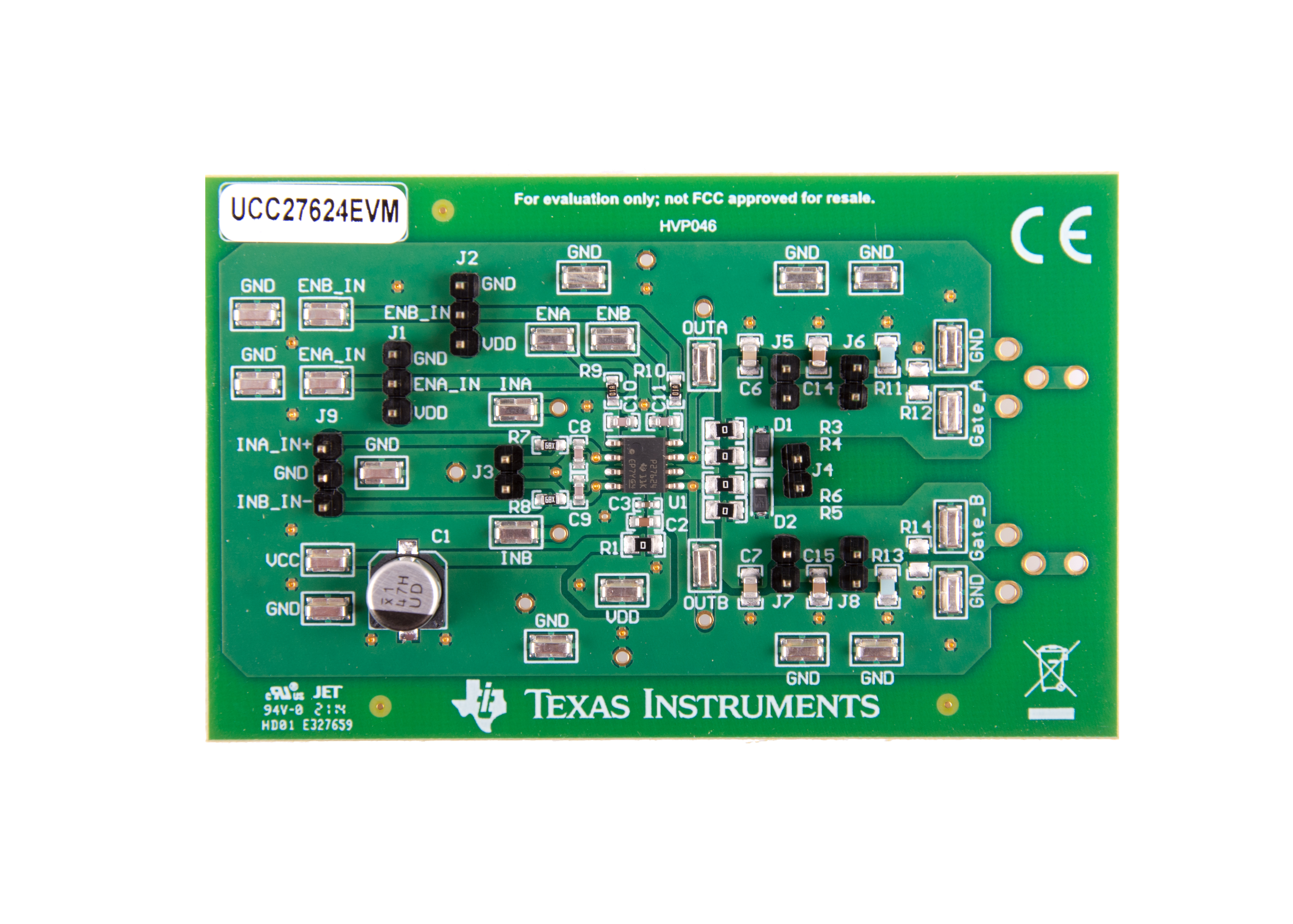
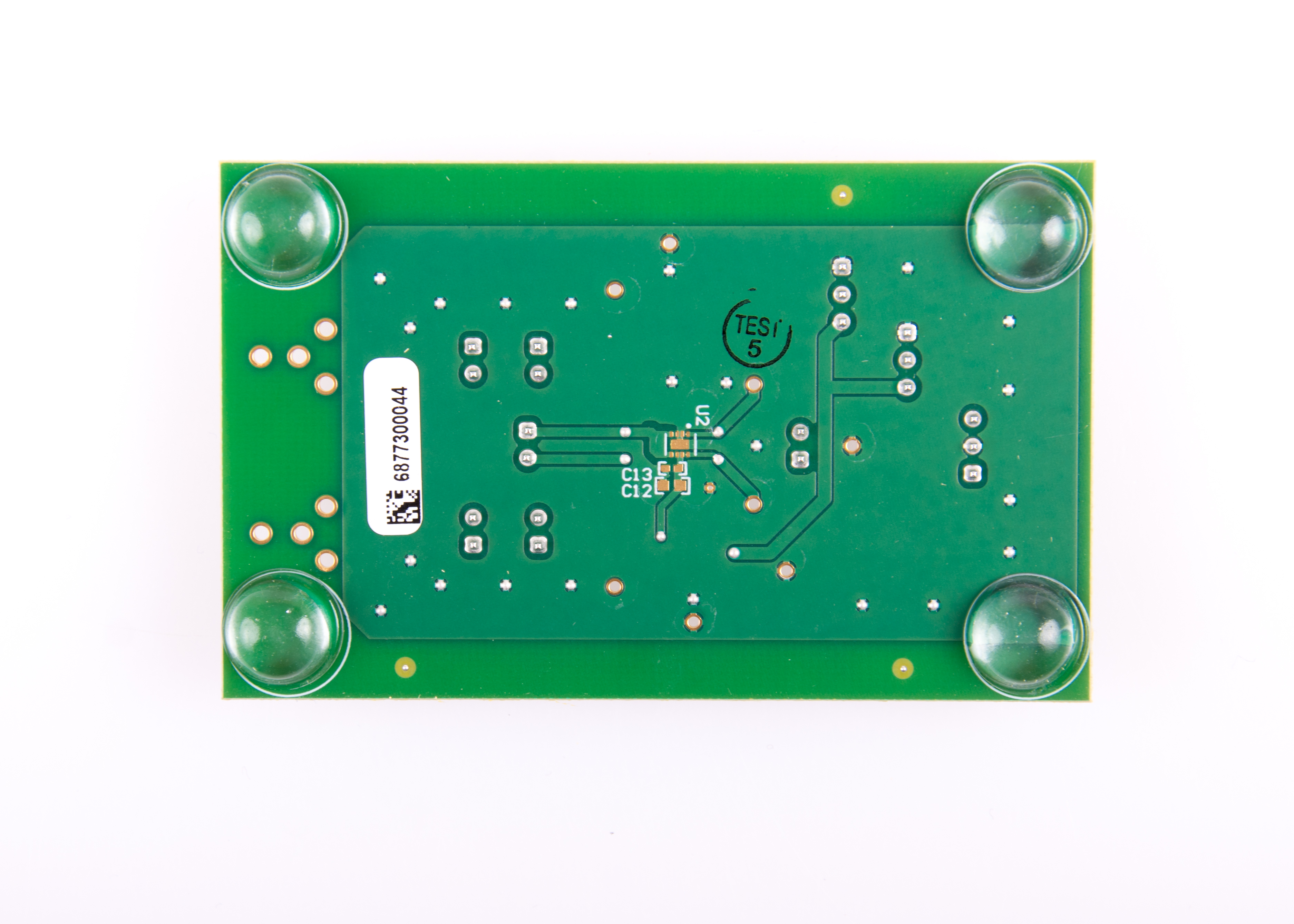
Figure 8-1 through Figure 8-6 show the PCB layout information for the UCC27624EVM.
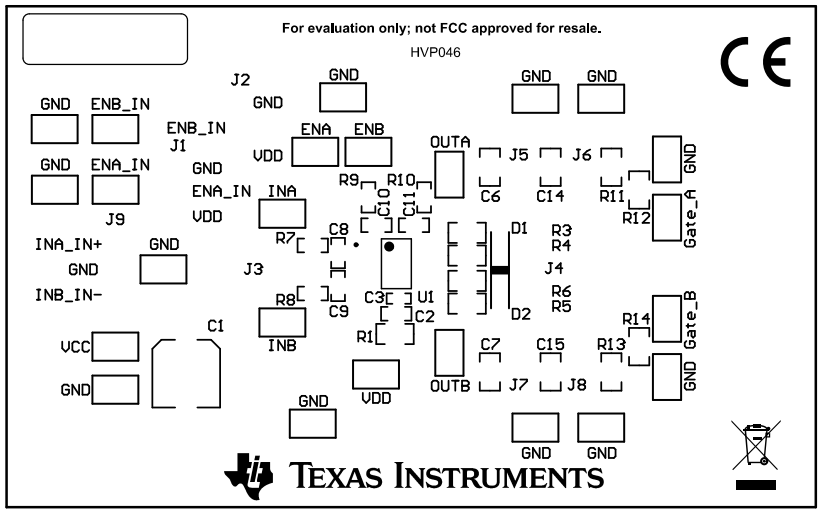
GUID-20210524-CA0I-KRPM-SSBR-DQPZBMJMC20C-low.pngFigure 8-1 Top Overlay
GUID-20210524-CA0I-G3V8-DMZ3-N07QWRR5Q9XG-low.pngFigure 8-2 Top Layer
GUID-20210524-CA0I-DC3P-4WSQ-JH9QMKKPMK3T-low.pngFigure 8-3 Bottom Layer
GUID-20210524-CA0I-QPMS-VDTF-8S01J5DWKKVG-low.pngFigure 8-4 Bottom Overlay
GUID-20210521-CA0I-KKBP-SD9K-XTFFM9RNVWBQ-low.jpg Figure 8-5 Top Image
GUID-20210521-CA0I-WVM1-TCJ2-HHCJNDZSK1ZN-low.jpg Figure 8-6 Bottom Image