SLUUCE9A December 2020 – April 2021 TPS543820 , TPS543820E
- Trademarks
- 1Introduction
- 2Configurations and Modifications
-
3Test Setup and Results
- 3.1 Input/Output Connections
- 3.2 Efficiency
- 3.3 Output Voltage Regulation
- 3.4 Load Transient and Loop Response
- 3.5 Output Voltage Ripple
- 3.6 Input Voltage Ripple
- 3.7 Synchronizing to a Clock
- 3.8 Start-up and Shutdown with EN
- 3.9 Start-up and Shutdown with VIN
- 3.10 Start-up Into Pre-Bias
- 3.11 Hiccup Current Limit
- 3.12 Overvoltage Protection
- 3.13 Thermal Performance
- 4Board Layout
- 5Schematic and Bill of Materials
- 6Revision History
3.6 Input Voltage Ripple
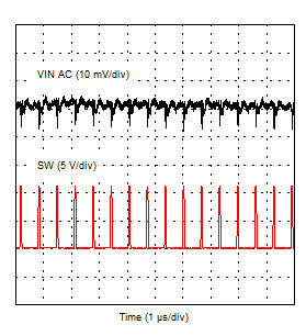
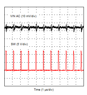
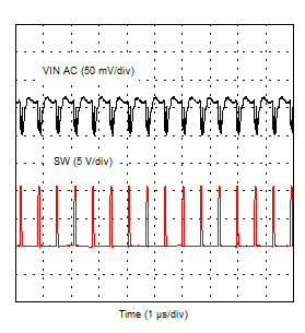
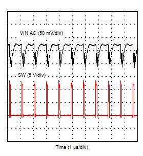
Figure 3-20 through Figure 3-23 show the TPS543820EVM input voltage ripple. The load currents are no load and 6 A. VIN = 12 V. The ripple voltage is measured across C1 for U1 and measured across C13 for U2.
 Figure 3-20 U1 Input Ripple
– No Load
 Figure 3-22 U2 Input Ripple – No Load
 Figure 3-21 U1 Input Ripple
– 6-A Load
 Figure 3-23 U2 Input Ripple – 6-A Load