SLUUCR5A december 2022 – june 2023 LM74900-Q1
6.1 PCB Drawings
Figure 6-1 and Figure 6-2 show component placement of the EVAL board. Figure 6-3 through Figure 6-6 show PCB layout images.
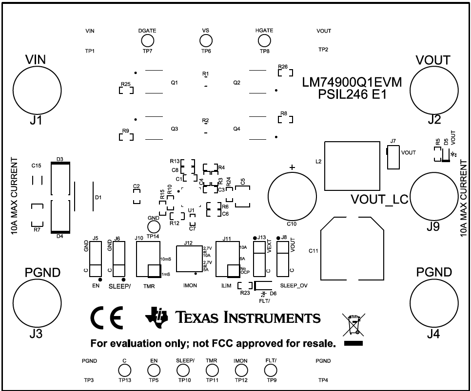 Figure 6-1 LM74900Q1EVM Board Top
Overlay
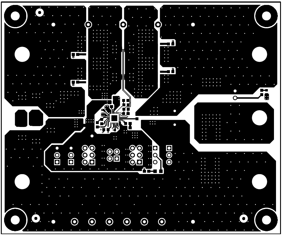 Figure 6-3 LM74900Q1EVM Board Top
Layer
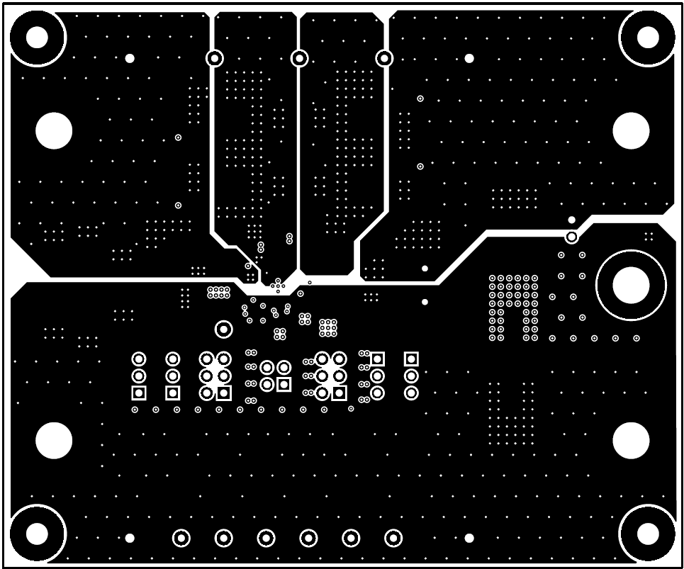 Figure 6-5 LM74900Q1EVM Board Inner
Layer 1
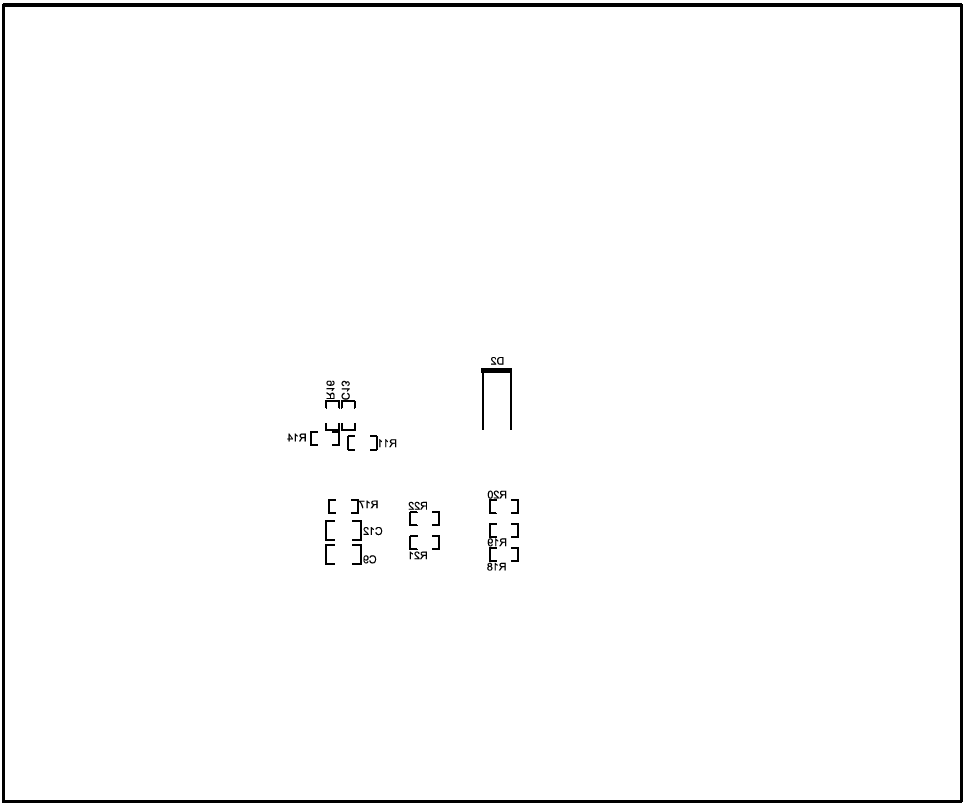 Figure 6-2 LM74900Q1EVM Board Bottom
Overlay
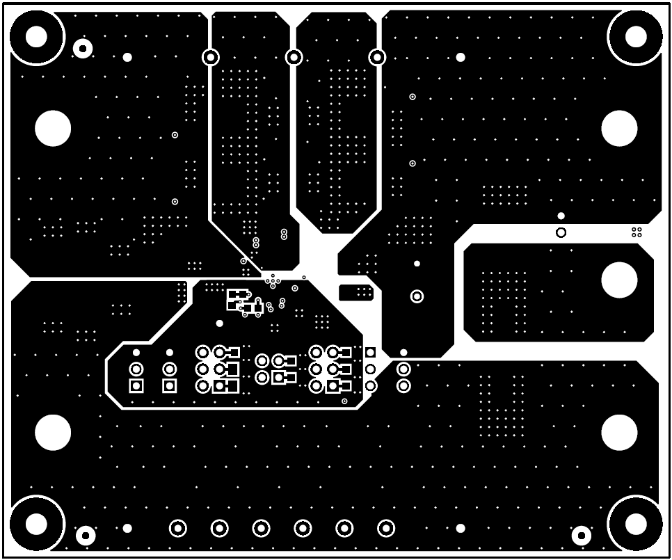 Figure 6-4 LM74900Q1EVM Board Bottom
Layer
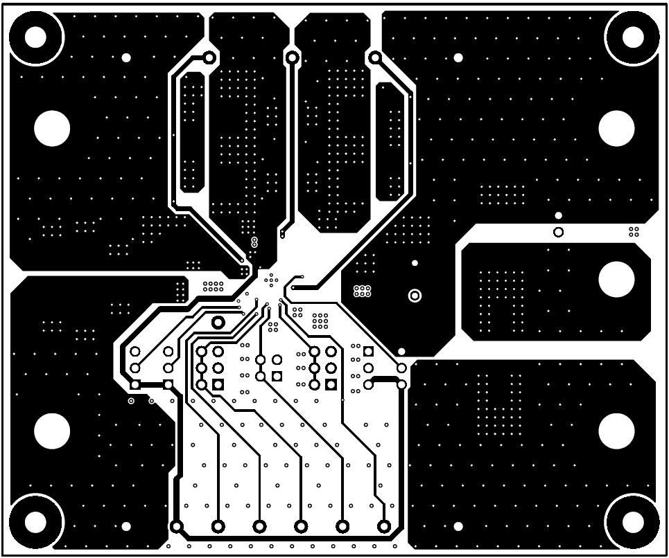 Figure 6-6 LM74900Q1EVM Board Inner
Layer 2