SLUUCS6A february 2023 – august 2023 UCC14340-Q1 , UCC14341-Q1
5.9.2 Output OVP of COM-VEE
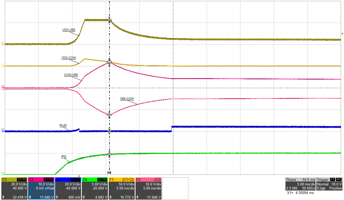
Figure 5-22 shows the effect of mismatched bias loading at startup where the load on VDD-COM is greater than the load on VEE-COM. A fixed resistive load of 620-Ω (188 mW @ VDD-COM=10.8 V) is applied to VDD-COM while VEE-COM is left unloaded. VDD-VEE is regulating at 22.4-V, as expected but VDD-COM is measuring 10.8 V (18-V setpoint) and VEE-COM is measuring 11.6 V (4-V setpoint). COM-VEE is directly monitored by FBVEE and has exceeded 110% of the set target value, triggering OVP and latching both outputs off, regardless of the 28.4-ms watch-dog-timer. Output OVP is allowed to exceed 110% of the targeted set value during start-up, prior to the /PG signal transitioning LOW. Otherwise, during steady state operation (/PG is LOW), if either feedback monitored output exceeds 110% of the set value, both outputs immediately shut down. When FBVEE has detected the regulated voltage exceeding the set target value, RLIM is internally switched to VEE, sinking current from the capacitor midpoint, COM connection. When activated, as illustrated in Figure 5-22, the outputs are latched off into a protected sate. EN or VIN must be recycled to clear the OVP fault and attempt to restart the module. The slow /PG signal rise time is a result of turning on the external EN (and /PG) power supply to turn on/off the EVM.

Figure 5-22 COM-VEE OVP: VIN=15 V, PVDD=188 mW, PVEE=0 mW, (top: VDD-VEE, 20 V/div, mid-1: VDD-COM, 50 V/div, mid-2: COM-VEE, 10 V/div, mid-3: VEE-COM, 10 V/div, mid-4: RLIM, 20 V/div, bot: /PG, 5 V/div), time = 5 ms/div
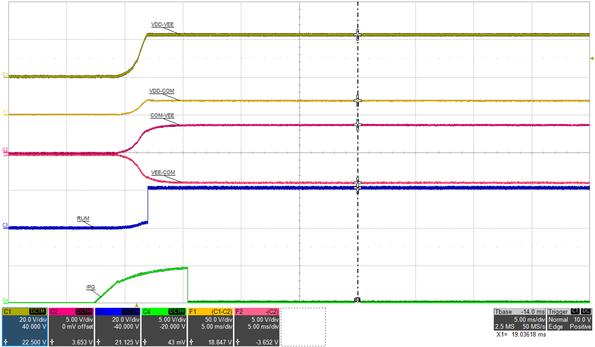
Figure 5-23 shows the same fixed resistive load of 620-Ω (573 mW) applied to VDD-COM as Figure 5-22 and the load on VEE-COM is the same 33-Ω (404 mW) as applied in Figure 5-22. VDD-VEE and COM-VEE are within their respective limits and the RLIM function is shown pulled HIGH to VDD-VEE attempting to compensate for the detected load differences. COM-VEE=3.6 V, which is near the minimum limit close to UVLO. Figure 5-23 demonstrates the EVM, as presently configured, is able to operate with up to 169 mW load difference (573 mW-404 mW). Changing the load on VDD-COM, VEE-COM, RLIM resistor value or capacitor value impacts how much load difference can be tolerated.

Figure 5-23 Normal Start (close to COM-VEE UVLO): VIN=15 V, PVDD=573 mW, PVEE=404 mW, (top: VDD-VEE, 20 V/div, mid-1: VDD-COM, 50 V/div, mid-2: COM-VEE, 5 V/div, mid-3: VEE-COM, 5 V/div, mid-4: RLIM, 20 V/div, bot: /PG, 5 V/div), time = 5 ms/div