SLUUCS6A
february 2023 – august 2023
UCC14340-Q1
,
UCC14341-Q1
1
Abstract
Trademarks
1
Introduction
1.1
U1 Component Selection
1.2
Pin Configuration and Functions
2
Description
2.1
EVM Electrical Performance Specifications
3
Schematic
4
EVM Setup and Operation
4.1
Recommended Test Equipment
4.2
External Connections for Easy Evaluation
4.3
Powering the EVM
4.3.1
Power on for Start-up
4.3.2
Power off for Shutdown
4.4
EVM Test Points
4.5
Probing the EVM
5
Performance Data
5.1
Efficiency Data
5.2
Regulation Data
5.3
Steady State Input Current
5.4
Start-up Waveforms
5.5
Inrush Current
5.6
AC Ripple Voltage
5.7
EN-to-/PG Timing
5.8
RLIM
5.9
Fault Protection
5.9.1
Output UVLO
5.9.2
Output OVP of COM-VEE
5.10
Shutdown
5.11
Thermal Performance
6
Assembly and Printed Circuit Board (PCB) Layers
7
Bill of Materials (BOM)
8
Revision History
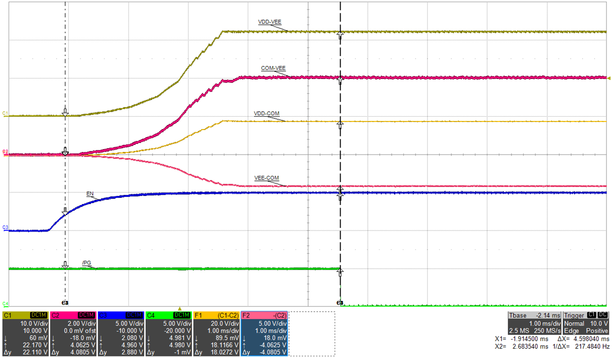
5.7
EN-to-/PG Timing
Figure 5-17
ENA to /PG Delay, 4.6 ms, VIN=15 V, I
VDD-VEE
=68 mA, (top: VDD-VEE, 10 V/div, mid-1: COM-VEE, 2 V/div, mid-2: VDD-COM, 20 V/div, mid-3: VEE-COM, 5 V/div, mid-4: EN, 5 V/div, bot: /PG, 5 V/div), time = 1 ms/div