SLUUCS7 april 2023 TPSM843A26
3.4 Load Transient and Loop Response
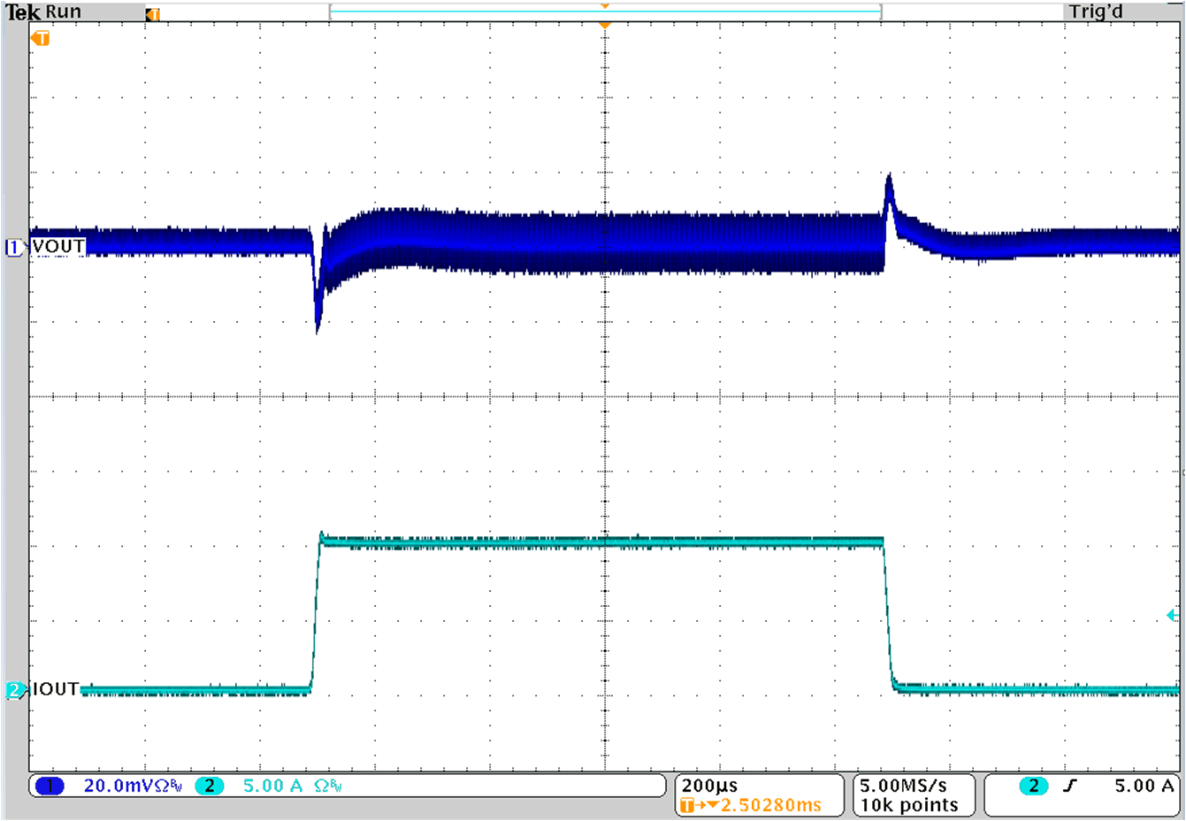
Figure 3-8 shows the load transient response. The current step is from 0 A to 10 A and the current step slew rate is 0.6 A/us. An electronic load is used to provide the step. The VOUT voltage is measured using J7 SMB connector.
Figure 3-9 shows the loop characteristic. Gain and phase plots are shown for VIN voltage of 12-V and 12-A and 16-A load.
 Figure 3-8 U1 Transient Response
 Figure 3-10 U1 Bode Plot – 16-A Load
 Figure 3-9 U1 Bode Plot – 12-A Load
Figure 3-11 and Figure 3-12 shows the loop characteristics for U1 with the three different ramp settings.
 Figure 3-11 U1 Loop Gain with Different Ramp Settings
 Figure 3-12 U1 Loop Phase with Different Ramp Settings