SLUUCT0A may 2023 – june 2023 TPS923652 , TPS923653 , TPS923654 , TPS923655
7 Layout
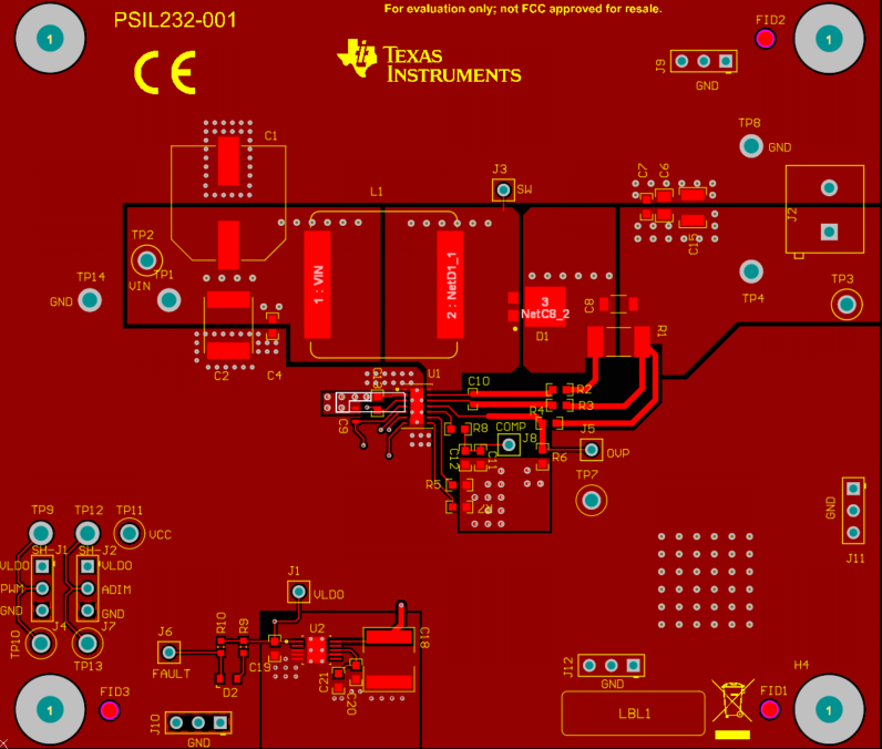
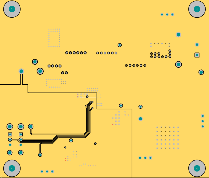
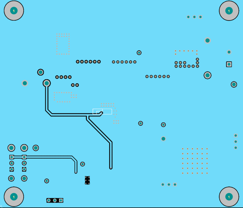
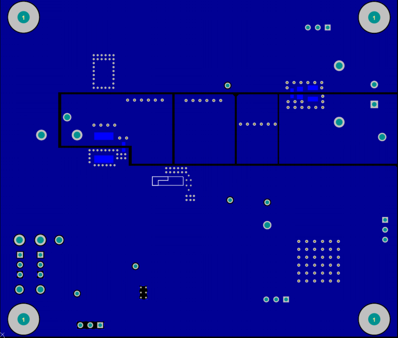
Figure 7-1, Figure 7-2, Figure 7-3 and Figure 7-4 show the layout of the TPS923655DMTREVM printed circuit board (PCB). The only difference between TPS923655DMTREVM, TPS923655DRRREVM and TPS923653DYYREVM PCB layout is the main LED driver IC.
 Figure 7-1 TPS923655DMTREVM Top Layer
 Figure 7-2 TPS923655DMTREVM Inner Layer 1
 Figure 7-3 TPS923655DMTREVM Inner Layer 2
 Figure 7-4 TPS923655DMTREVM Bottom Layer