SLUUCT3 August 2024 LMR51635
3.2 PCB Layouts
This section provides a description of the LMR51635EVM, board layout, and layer illustrations.
The board images are shown in LMR51635EVM Top ViewLMR51635EVM Front Photo and Figure 3-3. The board layouts are shown in Figure 3-4 to Figure 3-7. The PCB consists of a 4-layer design. The board size is 55mm × 57mm. 2oz copper planes are applied on top and bottom layers, 1oz copper planes are applied on middle layers.
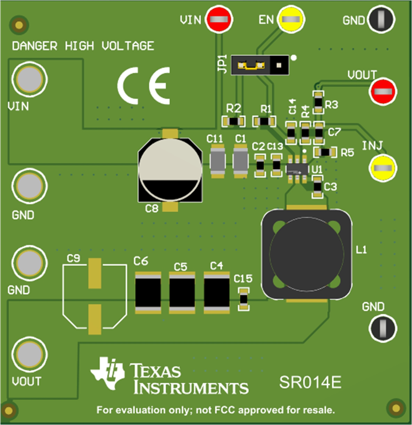 Figure 3-2 LMR51635EVM Front Photo
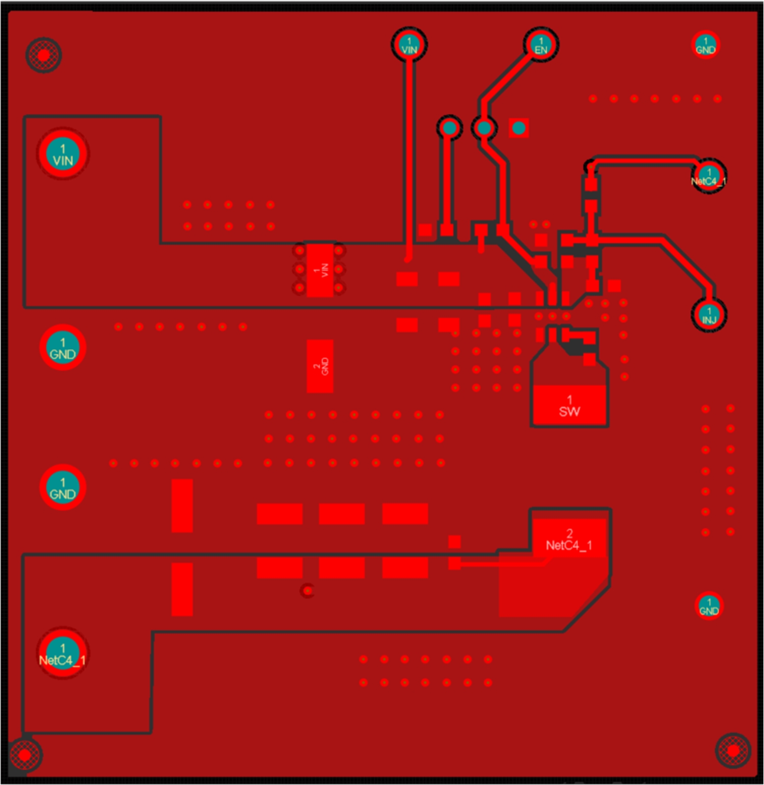 Figure 3-4 Top Layer
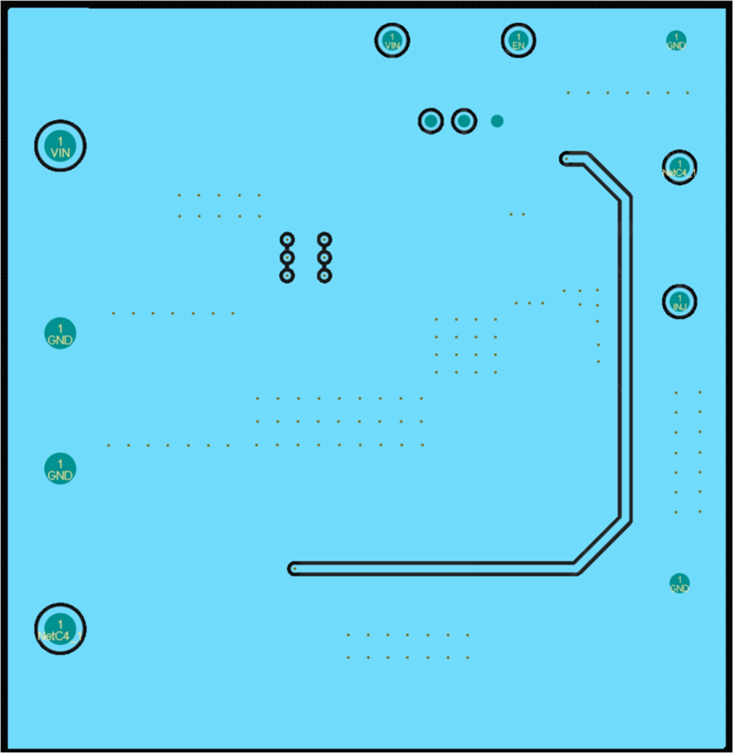 Figure 3-6 Middle Layer 2
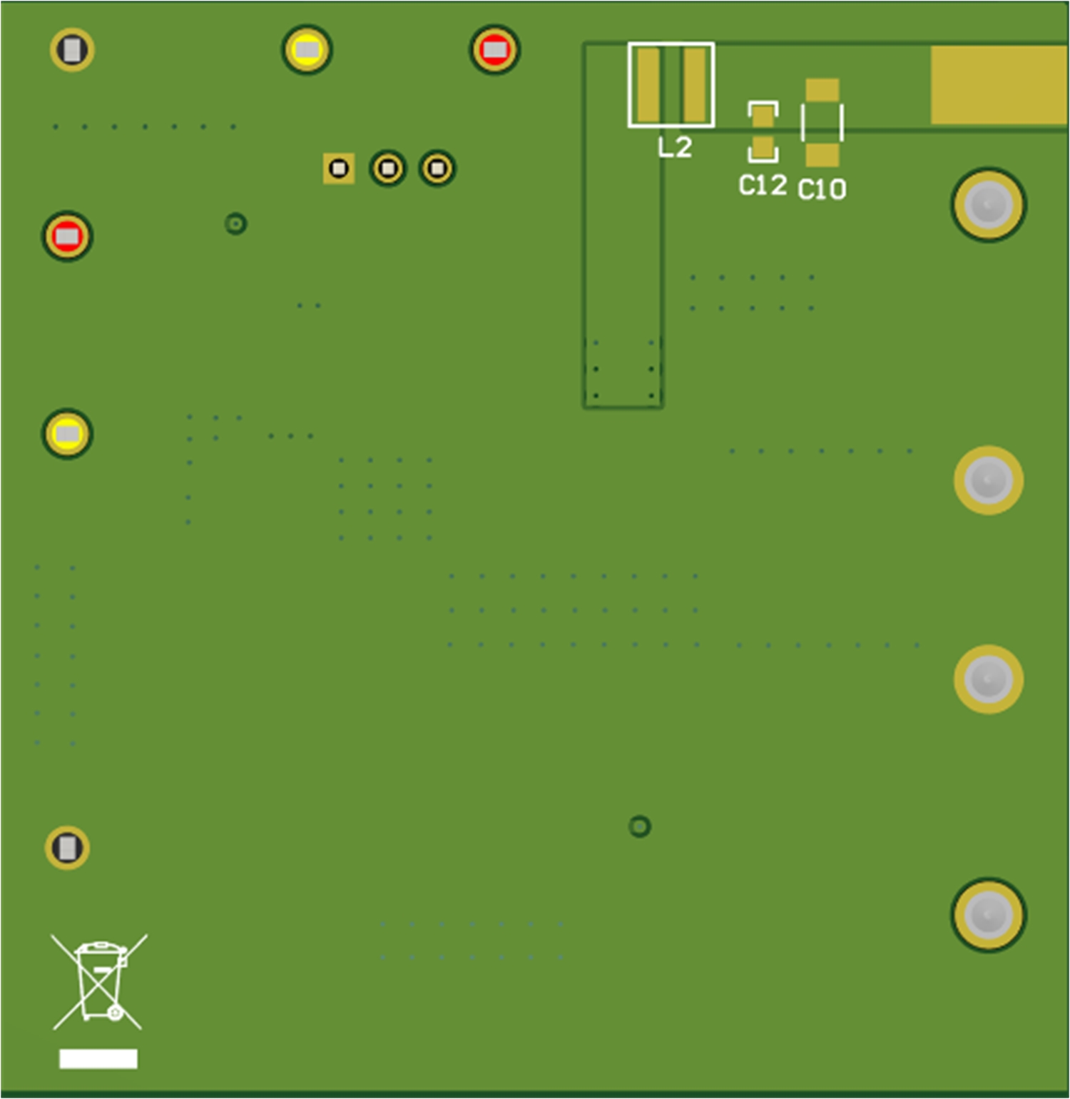 Figure 3-3 LMR51635EVM Back Photo
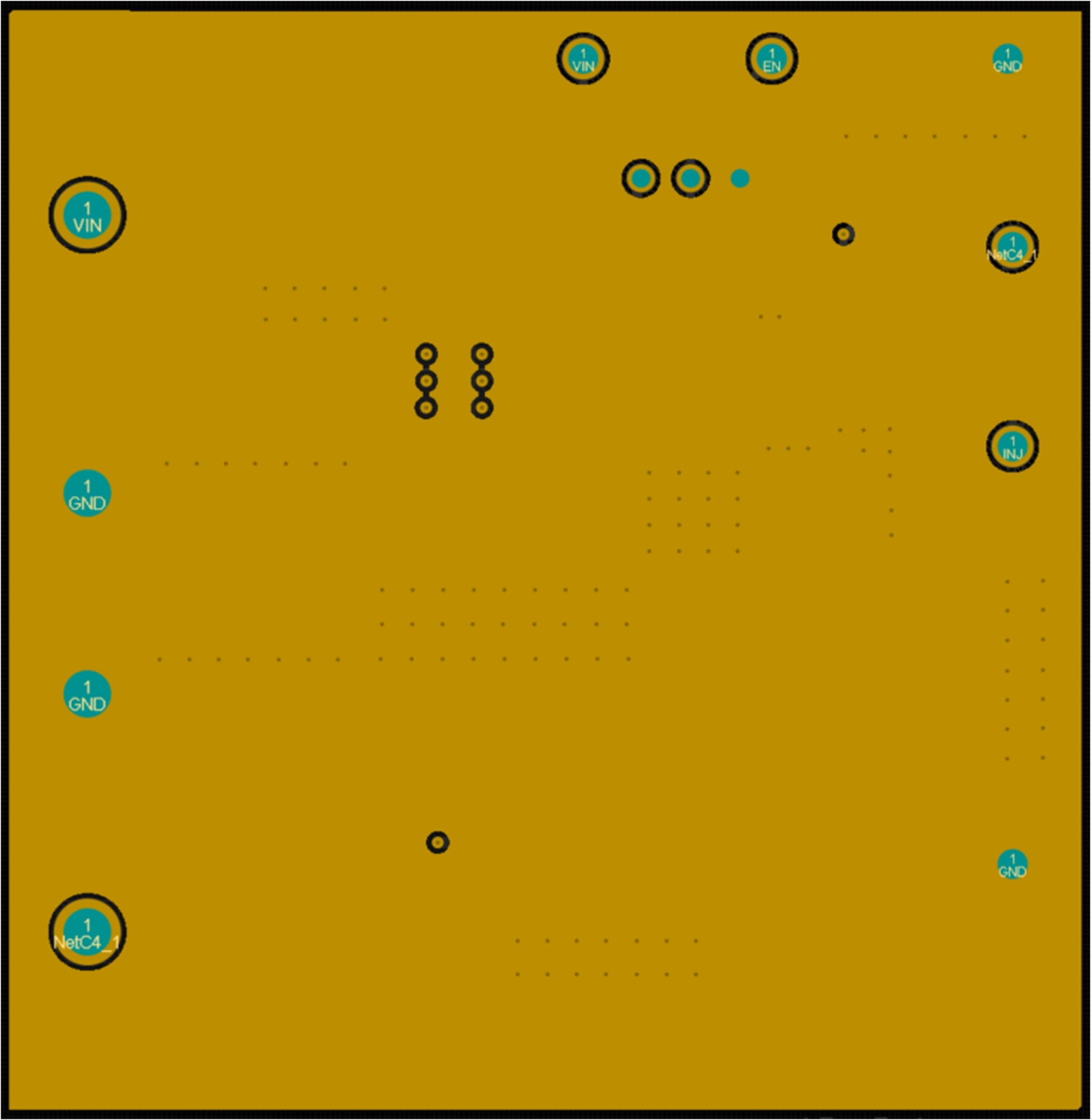 Figure 3-5 Middle Layer 1
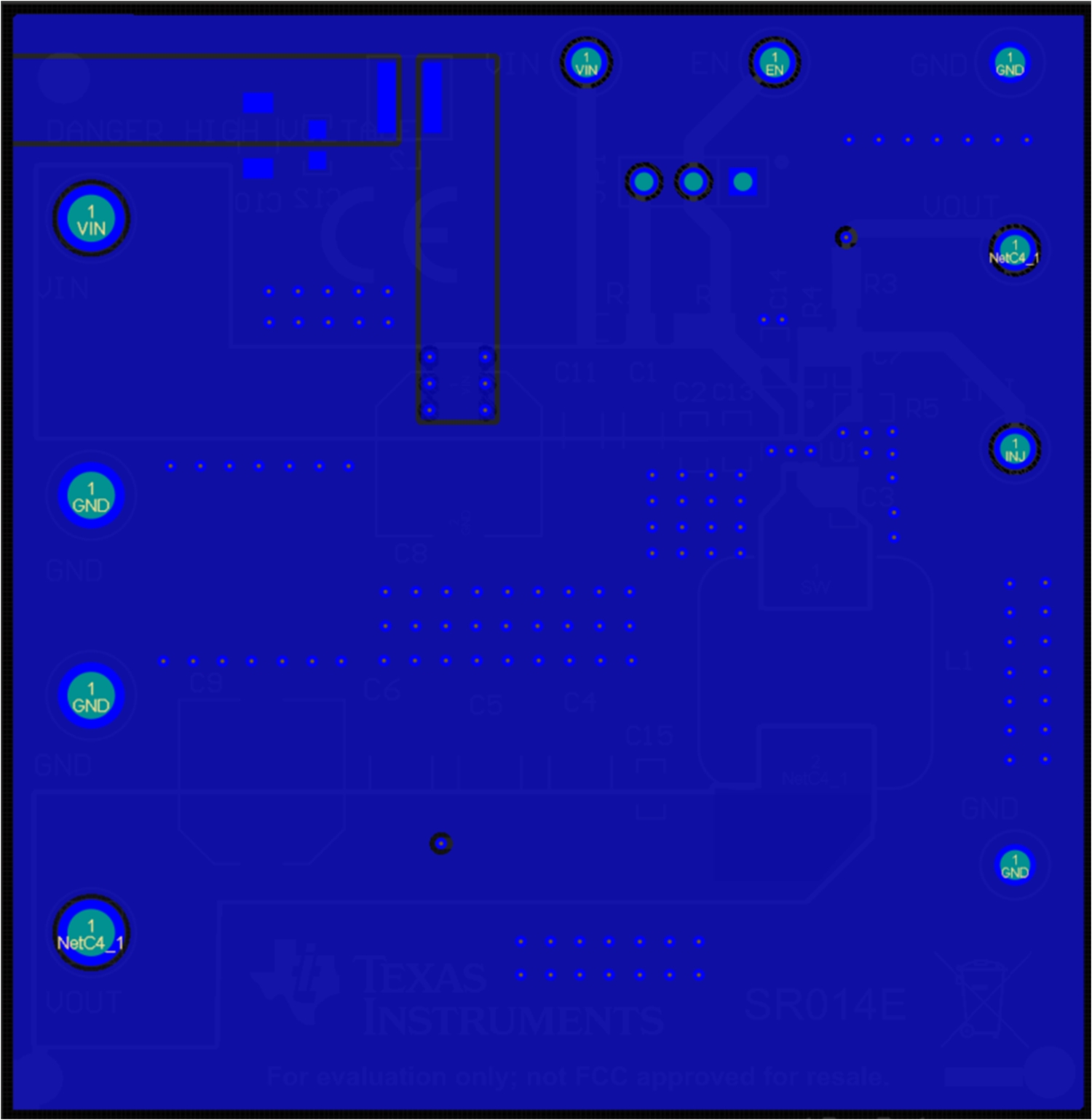 Figure 3-7 Bottom Layer