SLUUCT9 September 2023
3.2 Performance Data and Results
Test Procedure
- Power Up
- Before proceeding make sure the EVM and all equipment is setup as described in section Equipment Configurations and Equipment Setup.
- Turn on the 5 V and 24 V power supply. Probing VDDB(TP16)-VSSB(TP9) measures 20 V. Probing VCC1(TP1)-GND(TP6) measures 5 V.
- Turn on both channels of the function generator.
- Use any probe of choice to verify that there is a 5 KHz, 5 V, pulse on INA and INB each with respect to GND.
- Probing VGA-VSSA and VGB-VSSB shows a PWM output signal from the gate driver going up to +16V when HIGH and -3V when LOW as shown in Figure 4-2.
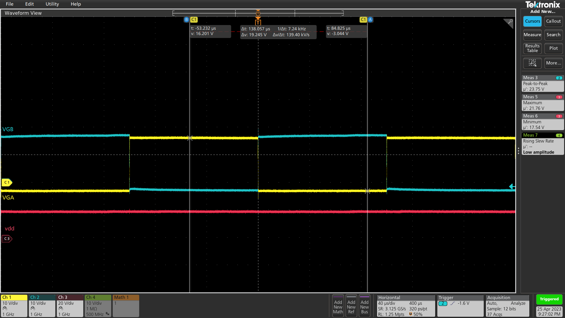 Figure 3-2 Power-up Test: Switching at 5 kHz
Deadtime Configuration
The UCC21551 has 3 dead time modes that are selectable with the UCC21551CQEVM. Those modes are Interlock, Programmable, and Overlap.
- Interlock Mode: Interlock mode sets a minimum delay of approximately 5 ns between gate driver outputs to prevent the channels from overlapping. This mode is initiated when the dead time pin is grounded (Shunting J5 to DT-GND). The dead time is defined as the delay between 90% of the falling edge of the first output and 10% of the rising edge of the second output. Timing is illustrated in Figure 4-3. See Figure 4-4for an example of Interlock mode.
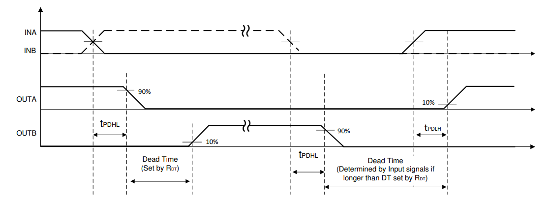 Figure 3-3 Timing Diagram
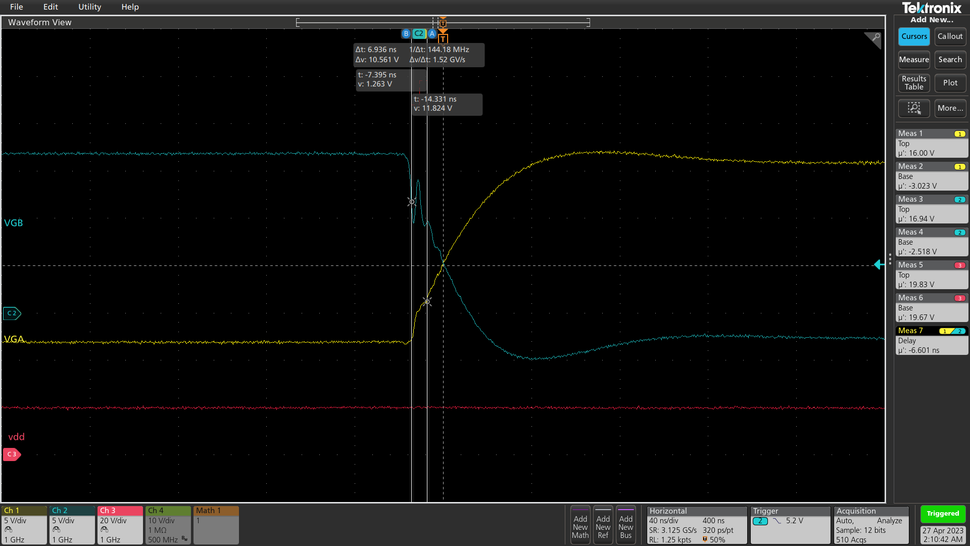 Figure 3-4 Interlock Mode
- Programmable Mode: Programmable dead time mode is activated when the dead time pin is connected to a resistor between 1.7K-100K Ohms to ground. To activate this mode on the EVM, leave jumper J5 unconnected. To adjust the deadtime, use the switches on SDT_DT1. By default, switch the switches to the left. To program the dead time, move the switch to the right. The available resistors allow for various dead time settings. Additional values can be created by toggling multiple switches at the same time, which has the effect of paralleling the resistors. Figure 4-5 is an example output waveform with 5 kΩ resistance.
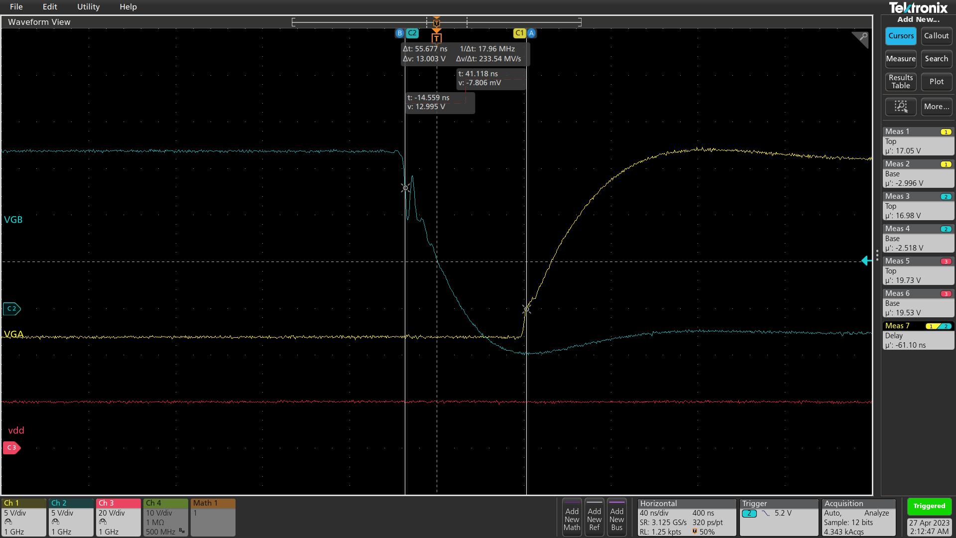 Figure 3-5 Programmable Mode: 5 kΩ RDT Resistor Selection
- Overlap Mode: Overlap mode disables the deadtime circuitry to allow the outputs to overlap. To select this mode, shunt jumper J5 to VCC-DT. An example of overlap mode is depicted in Figure 4-6.
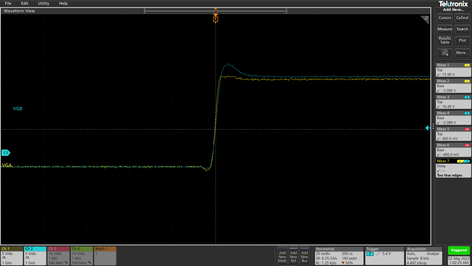 Figure 3-6 Overlap Mode
Single Input PWM
Single input PWM allows the user to control channel A and B with a single PWM signal. On the EVM, this is accomplished with a BJT inverter circuit that takes the incoming channel A signal inverts and forwards to the input pin of channel B. To enable this mode, shunt jumper 23. Note that in this mode, there is an unavoidable intrinsic dead time of 1us imposed by the BJT switching delay. This only occurs between the falling edge of VGA and the rising edge of VGB. If the deadtime circuit of the UCC21551 is enabled, then the interlock and programmable deadtime modes only affects the rising edge of VGA and the falling edge of VGB. This is because the 1us deadtime caused by the BJT is happening in parallel with the gate driver deadtime instead of adding. In Figure 4-7 and Figure 4-8, the driver is in interlock mode and both channels are switching at the same frequency. As the frequency increases, the output pulses eventually become smaller than the 1us delay. Figure 4-8 is depicting switching at 200 kHz, at which about half of INB’s signal is lost.
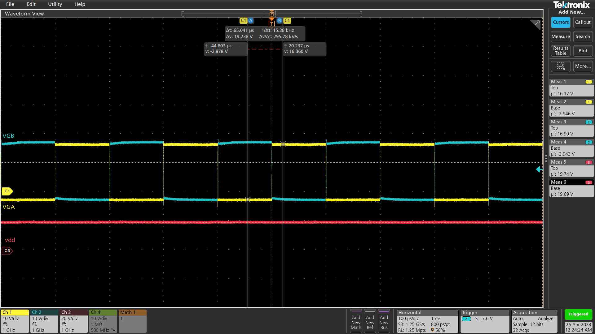 Figure 3-7 Switching at 5 kHz
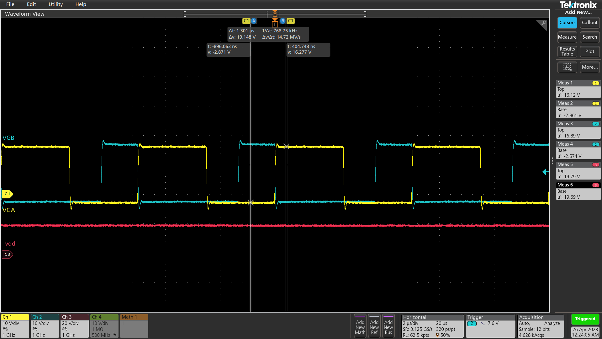 Figure 3-8 Switching at 200 kHz
Active Clamp
The Active clamp is a protection circuit added to channel B of the UCC21551CQEVM. This circuit helps keep the gate low when the driver is not powered or if there is an unintended voltage rise coupling to VGB. If there is a rise in the voltage on VGB greater than the voltage on OUTB, then the PNP BJT turns on and provides a path for current to flow to ground instead of into the FET gate, which can turn the FET on. The active clamp clamps voltage transients on VGB to approximately 1.2V. This is shown in Figure 4-9.
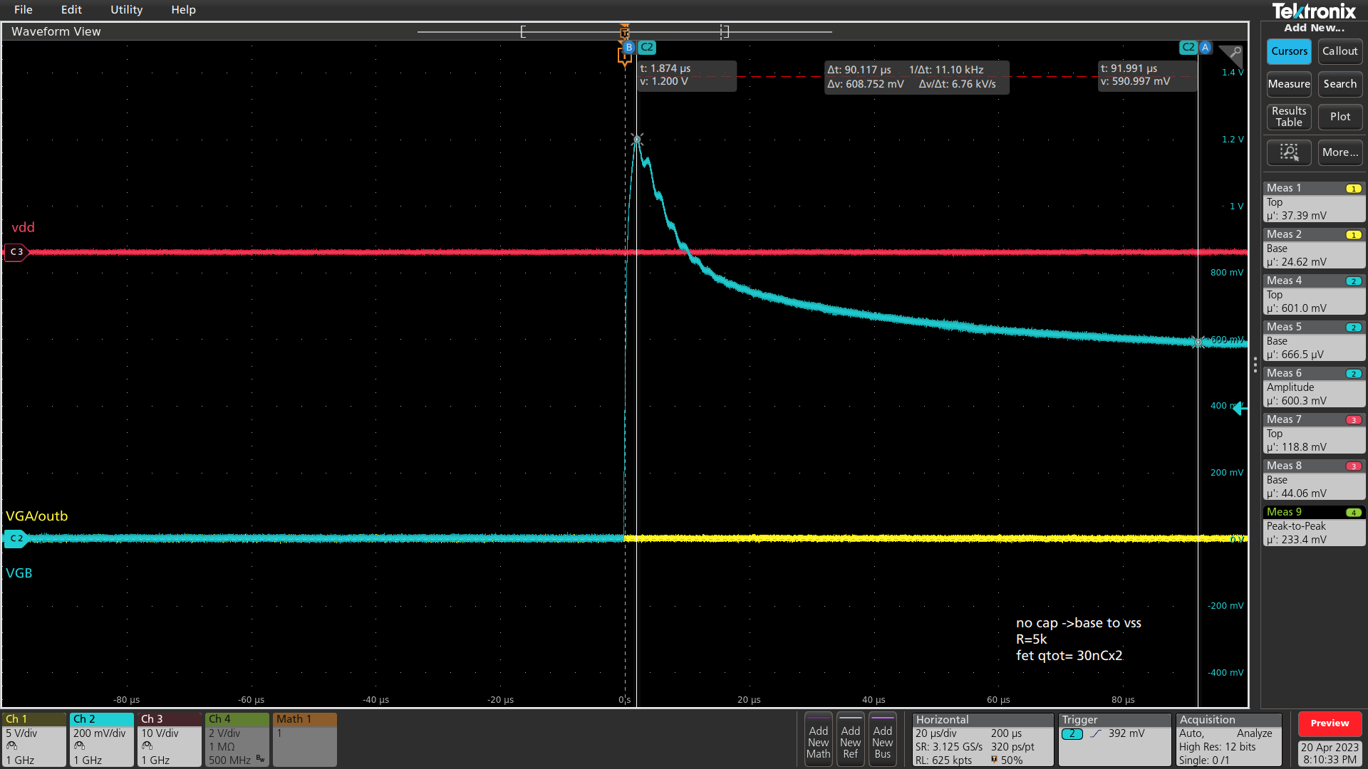 Figure 3-9 Active Clamp Clamping an Unintended Rise on VGB
Onboard Adjustable Bias Supply (UCC14240)
The UCC14240 is a 1.5W isolated adjustable bias supply configured to supply 20 V to the low side (channel B) of the gate driver. The user can change this output voltage to accommodate different versions of UCC2155XX drivers by changing resistor R28. For more information on how to adjust the output voltages, refer to the UCC14240-Q1 Component Calculator and the application note UCC14240-Q1 Simplifies HEV, EV, Bias Supply Design for Isolated Gate Drivers.
Negative Bias Supply Generation
The UCC21551CQEVM is equipped with a zener diode circuit on both gate driver output channels. This takes the 20 V VDD supply and splits into +16/-3V. Applying a negative bias to the gate of MOSFET mitigates the system from having unintentional turn on of the MOSFET caused by current flowing through the miller capacitor during high dv/dt switching. The negative pulldown circuit needs multiple cycles to reach steady state. Not all tests, such as a double pulse test, feature a negative voltage on the gate when performed.
High Voltage Double Pulse Test
This UCC21551CQEVM-079 was designed to work with voltages of up to 800 V. A low side double pulse test was performed to test the high voltage capability of the EVM. This test consisted of a Wolfspeed XM3 evaluation board which includes a SiC FET module and DC bus capacitor. The inductor is connected across the high side FET so the body diode can free-wheel the inductor current while the low side FET switches.
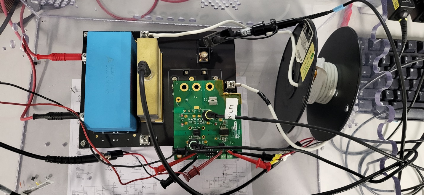 Figure 3-10 UCC21551CQEVM-079 Connected to SiC Wolfspeed XM3 Module
If the Wolfspeed XM3 evaluation board is not in use, then the user has the capability of connecting DC bus link capacitors to the board by using connectors J8 (DC+) and J12 (DC-).
Figure 4-11 shows the waveforms taken of an 800 V double pulse test. The signals are described below:
- Red: ID, inductor current
- Blue: Vds, drain to source voltage of the low side FET switching
- Yellow: Vg, gate voltage of the low side FET
- Green: Vin, channel B input pulse signal
The peak current measured during this test measured 522 amps and the peak voltage across the low side fet measured 977 volts.
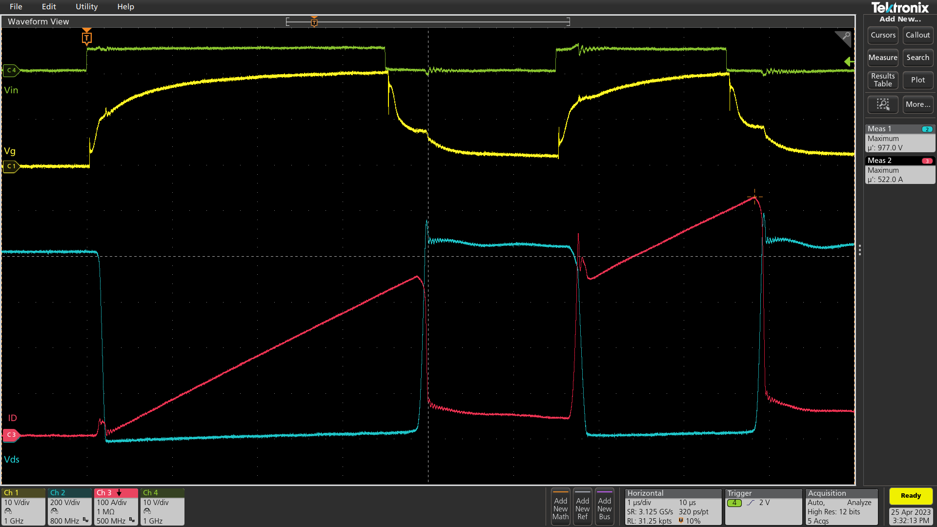 Figure 3-11 Double Pulse Test Results at 800 V