SLUUCU2A March   2023  – September 2023 UCC14130-Q1 , UCC14131-Q1


  1.   1
  2.   Abstract
  3.   Trademarks
  4. 1Introduction
    1. 1.1 U1 Component Selection
    2. 1.2 Pin Configuration and Functions
  5. 2Description
    1. 2.1 EVM Electrical Performance Specifications
  6. 3Schematic
  7. 4EVM Setup and Operation
    1. 4.1 Recommended Test Equipment
    2. 4.2 External Connections for Easy Evaluation
    3. 4.3 Powering the EVM
      1. 4.3.1 Power on for Start-up
      2. 4.3.2 Power off for Shutdown
    4. 4.4 EVM Test Points
    5. 4.5 Probing the EVM
  8. 5Performance Data
    1. 5.1  Efficiency Data
    2. 5.2  Regulation Data
    3. 5.3  Steady State Input Current
    4. 5.4  Start-Up Waveforms
    5. 5.5  Inrush Current
    6. 5.6  AC Ripple Voltage
    7. 5.7  EN and Timing
    8. 5.8  RLIM
    9. 5.9  Shutdown
    10. 5.10 Thermal Performance
  9. 6Assembly and Printed Circuit Board (PCB) Layers
  10. 7Bill of Materials (BOM)
  11. 8Revision History

Thermal Performance

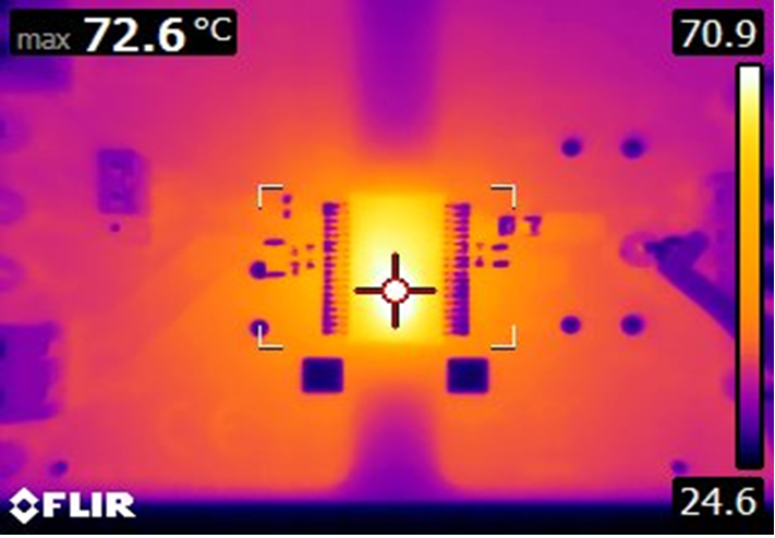
As shown in Figure 5-23, full load EVM operation can result in very hot U1 package temperature. Use caution not to touch the U1 case when probing or handling the EVM during full load operation.
GUID-D0E71F17-C289-4488-AEFC-39144BF807D1-low.png
VIN = 12 VVDD = 12 VIVDD = 128.5 mA
V+5V = 5.01 VI+5V = 0 mAPOUT = 1.54 W
TRISE = 48°C (see Equation 1)
Figure 5-23 VIN=12 V, IVDD = 128.5 mA, 1.54 W
GUID-20230320-SS0I-BRXT-RCFL-GJX4JBQPBHTT-low.svgFigure 5-24 Power Dissipation and Case Temperature vs Input Voltage, TA=24.6°C, 1.54 W
Equation 1. TRISE=72.6°C-24.6°C=48°C
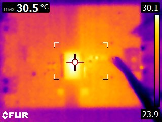
GUID-3BEEEA4A-D6D9-4885-B5EB-068E2455277D-low.png
VIN = 12 VVDD = 12 VIVDD = 0 mA
V+5V = 5.01 VI+5V = 0 mAPOUT = 0 W
TRISE = 6.6 °C (see Equation 2)
Figure 5-25 VIN=12 V, IVDD =0 mA, POUT=0 W
GUID-20230320-SS0I-PL41-XKZN-JCQC4FRQ0BJ8-low.svgFigure 5-26 Power Dissipation and Case Temperature vs Input Voltage, TA=23.9°C, 0 W
Equation 2. TRISE=30.5°C-23.9°C=6.6°C