SLUUCV8 October   2023 TPS4810-Q1


  1.   1
  2.   Description
  3.   Features
  4.   Applications
  5.   5
  6. 1Evaluation Module Overview
    1. 1.1 Introduction
    2. 1.2 Kit Contents
    3. 1.3 Specification
    4. 1.4 Device Information
  7. 2Hardware
    1. 2.1 Overview
    2. 2.2 General Configurations
      1. 2.2.1 Physical Access
      2. 2.2.2 Test Equipment and Setup
        1. 2.2.2.1 Power Supplies
        2. 2.2.2.2 Meters
        3. 2.2.2.3 Oscilloscope
        4. 2.2.2.4 Loads
  8. 3Implementation Results
    1. 3.1 Test Setup and Procedures
      1. 3.1.1 Power-up with EN Control
      2. 3.1.2 Overload and Short Circuit Protection Test
      3. 3.1.3 Short-Circuit Protection Diagnosis Test
      4. 3.1.4 Input Reverse Polarity Test
  9. 4Hardware Design Files
    1. 4.1 Schematic
    2. 4.2 PCB Layout
    3. 4.3 Bill Of Materials (BoM)
  10. 5Additional Information
    1.     Trademarks

PCB Layout

Figure 5-2 shows component placement of the EVAL Board, and Figure 5-4 and Figure 5-6 show PCB layout images.
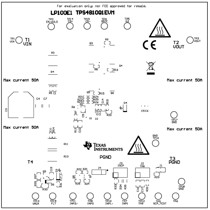
GUID-20231008-SS0I-44CL-QXQD-XWJLM5RJWBKC-low.pngFigure 4-2 TPS4810Q1EVM Board Top Overlay
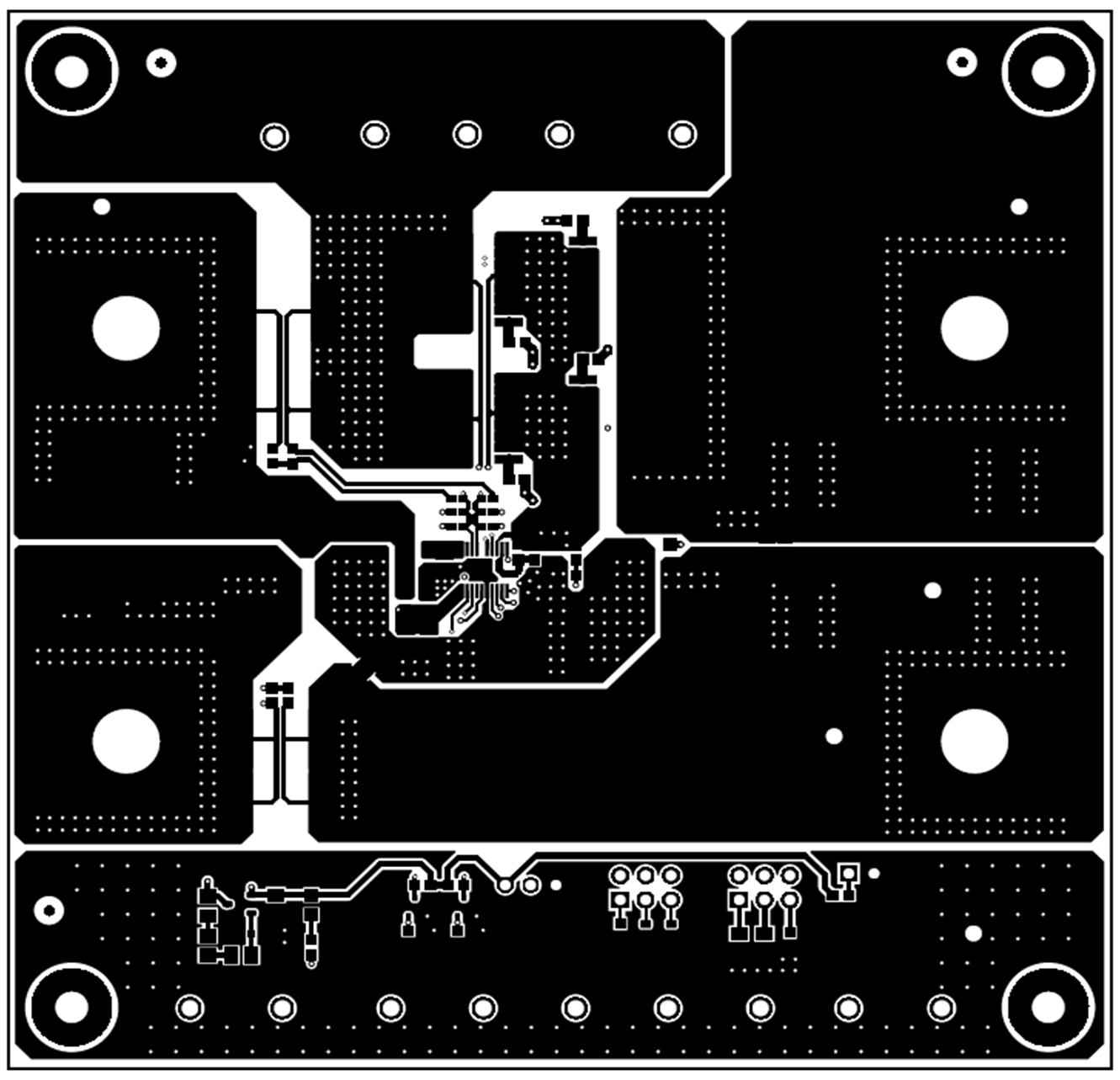
GUID-20231008-SS0I-97CQ-GQW0-2PJ4WG3BTBBF-low.pngFigure 4-4 TPS4810Q1EVM Board Top Layer
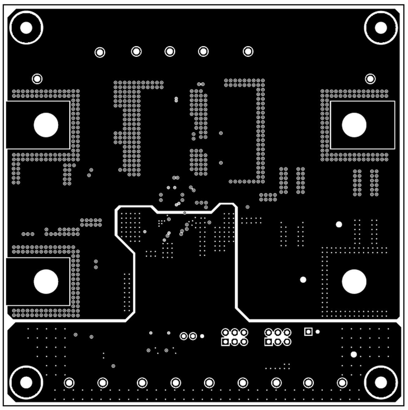
GUID-20231008-SS0I-D79F-DMCB-THQPQNCXQ4Q0-low.pngFigure 4-6 TPS4810Q1EVM Board Inner Signal Layer
GUID-20231010-SS0I-7KQW-ZK4H-G2K0L89K1X7N-low.pngFigure 4-3 TPS4810Q1EVM Board Bottom Overlay
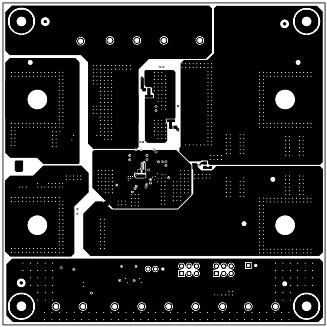
GUID-20231010-SS0I-GT17-1D6B-HJ3ZLLM9F8RD-low.pngFigure 4-5 TPS4810Q1EVM Board Bottom Layer
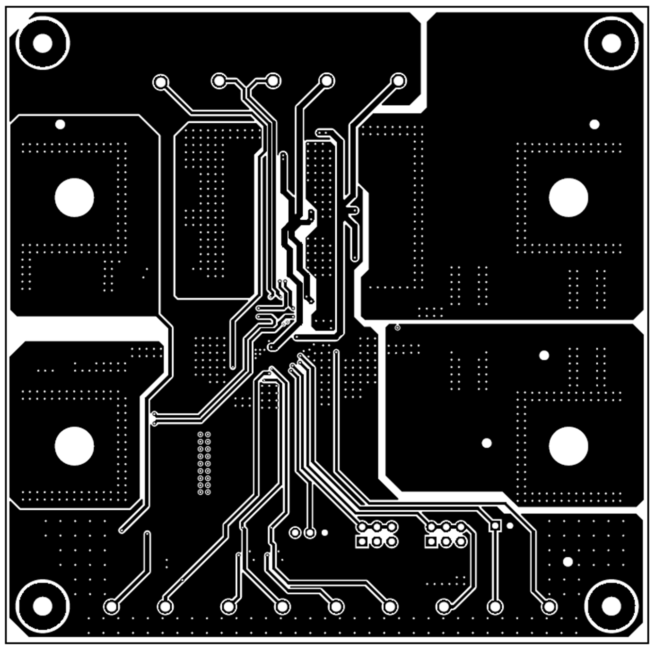
GUID-20231010-SS0I-1Q0Z-MZX2-4GX7W9CRZXBF-low.pngFigure 4-7 TPS4810Q1EVM Board Inner Routing Layer