SLUUCZ5 December   2024 TPS54538


  1.   1
  2.   Description
  3.   Features
  4.   Applications
  5.   5
  6. 1Evaluation Module Overview
    1. 1.1 Introduction
    2. 1.2 Kit Contents
    3. 1.3 Specification
    4. 1.4 Device Information
  7. 2Hardware
    1. 2.1 Test Setup and Procedure
      1. 2.1.1 EVM Connections
      2. 2.1.2 Test Equipment
      3. 2.1.3 Recommended Test Setup
        1. 2.1.3.1 Input Connections
        2. 2.1.3.2 Output connections
      4. 2.1.4 Test Procedure
        1. 2.1.4.1 Line and Load Regulation, Efficiency
  8. 3Implementation Results
    1. 3.1 Performance Data and Results
      1. 3.1.1 EVM Characteristics
      2. 3.1.2 Conversion Efficiency
      3. 3.1.3 Operating Waveforms
        1. 3.1.3.1 Start-Up and Shutdown with EN
        2. 3.1.3.2 Start-Up with VIN
        3. 3.1.3.3 Load Transient Response
        4. 3.1.3.4 Output Voltage Ripple
      4. 3.1.4 Thermal Performance
  9. 4Hardware Design Files
    1. 4.1 Schematic
    2. 4.2 PCB Layout
    3. 4.3 Bill of Materials
  10. 5Compliance Information
    1. 5.1 Compliance and Certifications
  11. 6Additional Information
    1. 6.1 Trademarks
  12. 7Related Documentation

PCB Layout

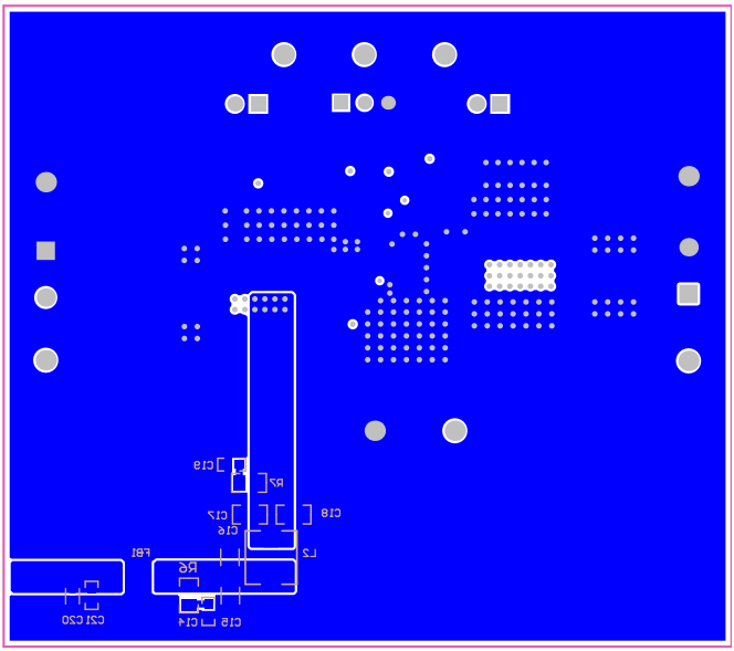
The design of the TPS54538EVM using a four-layer PCB with 2-oz copper thickness is shown in Figure 4-2 through Figure 4-5.
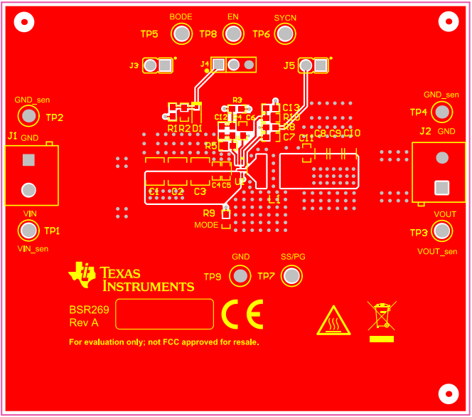
TPS54538EVM Top Copper (Top View)Figure 4-2 Top Copper (Top View)
TPS54538EVM Layer 3 Copper (Top View)Figure 4-4 Layer 3 Copper (Top View)
TPS54538EVM Layer 2 Copper (Top View)Figure 4-3 Layer 2 Copper (Top View)
TPS54538EVM Bottom Copper (Top View)Figure 4-5 Bottom Copper (Top View)