SLVA469D June 2013 – January 2023 TLV62130 , TLV62130A , TLV62150 , TLV62150A , TPS61175 , TPS61175-Q1 , TPS62130 , TPS62130A , TPS62131 , TPS62132 , TPS62133 , TPS62135 , TPS62136 , TPS62140 , TPS62140A , TPS62141 , TPS62142 , TPS62143 , TPS62150 , TPS62150A , TPS62151 , TPS62152 , TPS62153 , TPS62160 , TPS62161 , TPS62162 , TPS62163 , TPS62170 , TPS62171 , TPS62172 , TPS62173
2.3.1 Digital Input Pins (EN, FSW, DEF)
Because VOUT is the IC ground in this configuration, the EN pin must be referenced to VOUT instead of the ground. In a buck configuration, the specified typical threshold voltage for the enable pin in the product data sheet is 0.9V to be considered high and 0.3V to be considered low (see the TPS62130, TPS62140, TPS62150, TPS62160, and TPS62170 product data sheets, Reference 2 through Reference 6). In the inverting buck-boost configuration, however, the VOUT voltage is the reference; therefore, the high threshold is 0.9V + VOUT and the low threshold is 0.3V + VOUT. For example, if VOUT = -3.3V, the VEN is considered a high level for voltages above –2.4V and a low level for voltages below –3V. The same effect is true with the DEF and FSW pins.
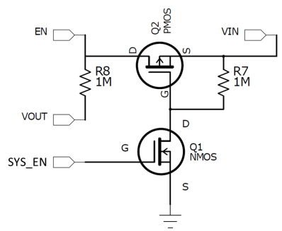
This behavior can cause difficulties enabling or disabling the part, since in some applications, the IC providing the EN signal may not be able to produce negative voltages. The level shifter shown in Figure 2-4 alleviates any problems associated with the offset EN threshold voltages by eliminating the need for negative EN signals.

The positive signal that originally drove EN is instead tied to the gate of Q1 (SYS_EN). When Q1 is off (SYS_EN grounded), Q2 sees 0V across its VGS, and also remains off. In this state, the EN pin sees VOUT which is below the low level threshold and disables the device.
When SYS_EN provides enough positive voltage to turn Q1 on (minimum VGS as specified in the MOSFET’s data sheet), the gate of Q2 is pulled low through Q1. This drives the VGS of Q2 negative and turns Q2 on. As a consequence, VIN ties to EN through Q2 and the pin is above the high level threshold, causing the device to turn on. Ensure that the VGD of Q2 remains within the MOSFET’s ratings during both enabled and disabled states. Failing to adhere to this constraint can result in damaged MOSFETs.
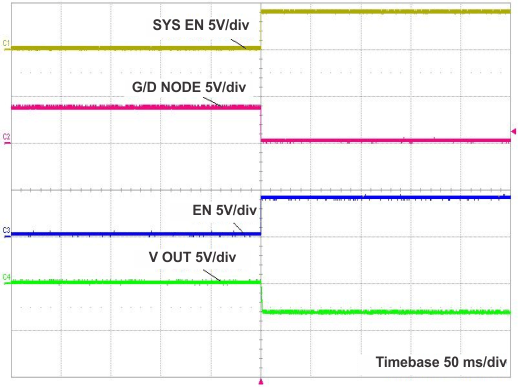
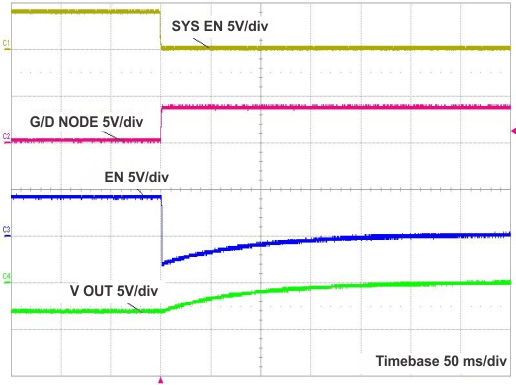
The enable and disable sequence is illustrated in Figure 2-5 and Figure 2-6. The SYS_EN signal activates the enable circuit, and the G/D NODE signal represents the shared node between Q1 and Q2. The EN signal is the output of the circuit and goes from VIN to –VOUT properly enabling and disabling the device. An active discharge circuit was implemented to accelerate –VOUT’s return to 0V when the IC is disabled.
 Figure 2-5 EN Pin Level Shifter on Startup
 Figure 2-6 EN Pin Level Shifter on Shutdown