Using the TPS62125 in an Inverting Buck-Boost Topology
1 Using the TPS62125 in an Inverting Buck-Boost Topology
The TPS62125 3-V to 17-V, 300-mA Step-Down Converter With Adjustable Enable Threshold and Hysteresis data sheet is a DCS-Control™ topology synchronous buck dc-to-dc converter designed for low-power applications. It features a wide operating input voltage range from 3 V to 17 V, 300-mA output current, and adjustable output voltage of 1.2 V to 10 V. This device is well-suited for applications such as ultra low-power microprocessors, energy harvesting, and low-power RF applications. Even though the TPS62125 can be configured in an inverting buck-boost topology, where the output voltage is inverted or negative with respect to ground. This application note describes the TPS62125 in an inverting buck-boost topology for use in low current negative rails for operational amplifier or optical module biasing and other low-power applications.
Trademarks
DCS-Control™ is a trademark of Texas Instruments.
All trademarks are the property of their respective owners.
1 Inverting Buck-Boost Topology
1.1 Design Considerations
The TPS62125 for inverting buck-boost application is very risky. We strongly recommend using our new generation buck converter TPS629203 or -Q1 family (including TPS629206 or -Q1 and TPS629210 or -Q1) instead of the TPS62125 for inverting buck-boost applications. The TPS629203 family not only has a higher current limit threshold, but most importantly, it does not require the inductor current to fall to zero before starting a new switching cycle. For example TPS629203 family has 0.9A typ. low-side current limit threshold, thus, the device will continue to switch as long as the DC bias current of downstream circuitry is below this 0.9A typ. threshold. More detailed information for TPS629203 inverting buck-boost application can be found in Using the TPS629210-Q1 in an Inverting Buck-Boost Topology.
The TPS62125 integrates a high-side MOSFET current limit ILIMF to protect the device against over current or short circuit fault. The current in high-side MOSFET is monitored by current limit comparator and once the current reaches the limit of ILIMF, the high-side MOSFET is turned off and low-side MOSFET is turned on to ramp down the inductor current. The high-side MOSFET is turned on again once zero current comparator trips and the inductor current has become zero.
The inverting buck-boost application is most commonly used to drive differential (+V/-V) rails. At some scenarios, the downstream devices become active as soon as the input voltage is present, their Iq current feeds into the negative (-V) rail even if the negative (-V) rail is not being enabled. There is a positive DC bias voltage is likely existed on the negative (-V) rail, then TPS62125 is more prone to get stuck as it may never see a zero-crossing current while getting into an over current fault due to this positive DC bias voltage.
A possible workaround solution for TPS62125 in inverting buck-boost application: Adjust the system power up sequence to prevent the downstream devices from loading the negative (-V) rail prior to the negative rail being enabled. That means to enable the negative (-V) rail first and then enable other downstream devices. Otherwise, TPS62125 probably gets stuck during power up.
1.2 Concept
The inverting buck-boost topology is very similar to the buck topology. In the buck configuration shown in Figure 1-1, the positive connection (VOUT) is connected to the inductor and the return connection is connected to the integrated circuit (IC) ground. However, in the inverting buck-boost configuration shown in Figure 1-2, the IC ground is used as the negative output voltage pin (labeled as –VOUT ). What used to be the positive output in the buck configuration is used as the ground (GND). This inverting topology allows the output voltage to be inverted and always lower than the ground.
 Figure 1-1 TPS62125 Buck Topology
 Figure 1-2 TPS62125 Inverting Buck-Boost Topology
The circuit operation is different in the inverting buck-boost topology than in the buck topology. Figure 1-3 (a) illustrates that the output voltage terminals are reversed, though the components are wired the same as a buck converter. During the on time of the control MOSFET, shown in Figure 1-3 (b), the inductor is charged with current while the output capacitor supplies the load current. The inductor does not provide current to the load during that time. During the off time of the control MOSFET and the on time of the synchronous MOSFET, shown in Figure 1-3 (c), the inductor provides current to the load and the output capacitor. These changes affect many parameters as described in the upcoming sections.
 Figure 1-3 Inverting Buck-Boost Configuration
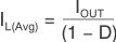
1.3 Output Current Calculations
The average inductor current is affected in this topology. In the buck configuration, the average inductor current equals the average output current because the inductor always supplies current to the load during both the on and off times of the control MOSFET. However, in the inverting buck-boost configuration, the load is supplied with current only from the output capacitor and is completely disconnected from the inductor during the on time of the control MOSFET. During the off time, the inductor connects to both the output cap and the load (see Figure 1-3). Knowing that the off time is 1 – D of the switching period, then the average inductor current is:
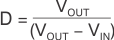
The duty cycle for the typical buck converter is simply VOUT / VIN but the duty cycle for an inverting buck-boost converter becomes:
Finally, the maximum inductor current becomes:
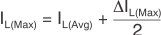
Where,
D: Duty cycle
∆IL (A): Peak to peak inductor ripple current
VIN (V): Input voltage with respect to ground, instead of IC ground or –VOUT.
The TPS62125’s current limit technique allows a simple maximum output current calculation. If the current exceeds ILIMF (the high-side MOSFET current limit), the high-side MOSFET switch turns off and the low-side MOSFET switch turns on until the inductor current ramps down to 0. If an overload is still present after reaching 0 current, the low-side MOSFET switch turns off and the high-side MOSFET switch turns on until current limit is reached again. In current limit, the inductor’s current goes from ILIMF to 0—its ripple current becomes ILIMF. Operating the TPS62125 in this state (with IL(Max) equal to ∆IL(Max) equal to ILIMF) reduces the average inductor current to ½ ILIMF (from Equation 3). With the TPS62125's minimum current limit value of 600 mA, this gives an IL(Avg) of 300 mA when current limit is reached. With this, the maximum allowable output current is calculated from Equation 1 and Equation 2, with a 5-V input voltage to –5-V output voltage system as an example:
D = –5 / (–5 – 5) = 0.5
This result is then used in Equation 1:
IOUT = IL(Avg) × (1 – D) = 300 × (1 – 0.5) = 150 mA
Due to increased duty cycles when operating at either lower input voltages (≤ 5 V) or with higher ambient temperatures (for example, at 85°C), the duty cycle used for the maximum output current calculation above should be increased by 10% for these conditions. This provides a more accurate maximum output current calculation. For the given example of a 5-V input and –5-V output, the maximum output current is then 300 x (1 - 0.6) = 120 mA.
The maximum output current for –5-V, –3.3-V and –8-V output voltages at different input voltages is displayed in Figure 1-4 and accounts for the above duty cycle increase for lower input voltages. Operation at higher temperatures would decrease the maximum output current shown for input voltages above 6 V as well.
 Figure 1-4 Maximum Output Current versus Input Voltage