-
Typical Design Guidelines for TPS92630/8-Q1 in Automotive Rear Lamp Applications SLVAEF0 September 2020 – MONTH TPS92630-Q1 , TPS92638-Q1
-
Typical Design Guidelines for TPS92630/8-Q1 in Automotive Rear Lamp Applications
Typical Design Guidelines for TPS92630/8-Q1 in Automotive Rear Lamp Applications
Trademarks
All other trademarks are the property of their respective owners.
1 Introduction
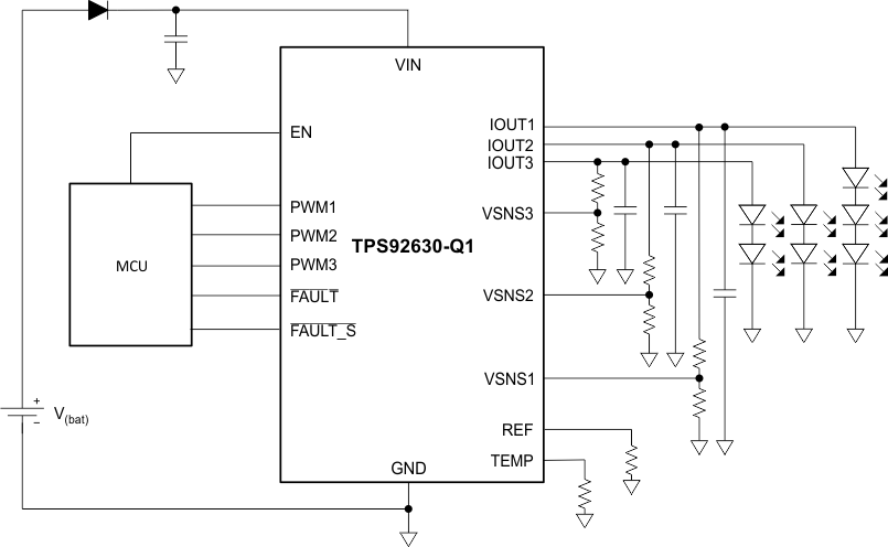
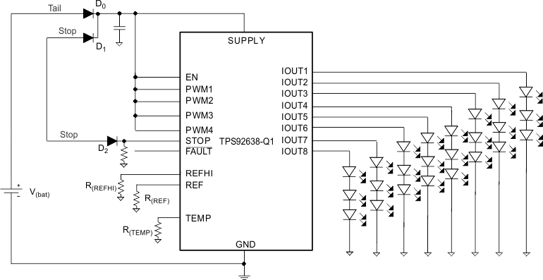
Figure 1-1 and Figure 1-2 shows the typical application schematics of the two devices. The VIN pin for TPS92630-Q1 and the SUPPLY pin for TPS92638-Q1 are power supply input pins. The voltage of the supply pins are expressed as V(supply) hereinafter. The supported supply voltage range of TPS92630/8-Q1 is 5 V - 40 V.
 Figure 1-1 TPS92630-Q1 Typical Application Schematic
 Figure 1-2 TPS92638-Q1 Typical Application Schematic
Both devices have full-diagnostic and built-in protection capabilities, such as output short-to-ground detection, open-load detection and reference resistor short detection. The fault detection features are effective when the device is enabled (V(EN) > 2 V).
2 Supply Line Transients In Automotive Rear Lamp Applications
In automotive equipments, the electric systems or components may be subjected to different supply line transients such as momentary drop in supply voltage, cold cranking, load dump, which can cause supply voltage deviations from the nominal values. Multiple tests, as specified in international standards such as ISO 7637-2 or ISO 16750-2, or specified by the the vehicle manufacturers, should be performed to evaluate the immunity of a device against these power supply transients.
In some transient scenarios, there is big voltage drop in power supply voltages. The V(supply) voltage seen at the power supply pins of TPS92630/8-Q1 may have different conditions, depending on the transient waveforms and the external circuits connected at the power supply pins.
According to the minimum value V(supply) decreases to, the device behavior can be divided into three different conditions, as shown in Figure 2-1. When V(supply) is always higher than 5 V and the device is enabled during the transient, the device keeps working in the normal state. When V(supply) decreases below 1.2 V or the device is disabled, the device will enter power-on-reset state where it will be reset. If V(supply) is between the two voltage levels and the device is enabled, the device behavior is undefined. The fault detection circuits may not be able to keep normal operation. Fault might be falsely detected and reported. If the device detects certain faults it falls into the protection mode and requires a power-on-reset to regain full functionality. So this condition should be avoided.
 Figure 2-1 Supply Voltage Conditions
If a V(supply) > 5 V cannot be guaranteed by the design and no other means of reset after faults (e.g. an MCU) are implemented, the following circuitry described in Section 3 can be used to ensure that the device is disabled when V(supply) is lower than 5 V, so that there will be no unwanted behavior triggered.
3 Recommended Circuit For Device Enable Control
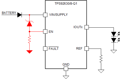
A recommended practical circuit to disable the device according to the power supply voltage is shown in Figure 3-1. A Zener diode is connected between V(supply) and EN and a resistor is connected from EN pin to ground to set a proper working current for the Zener diode.
 Figure 3-1 Recommended EN Control Circuit
The EN pin logic input threshold is shown in Table 3-1. Select a Zener diode with which you can ensure that the EN pin is lower than 0.7 V when V(supply) is lower than 5 V in order to shut down the device. And the device can be enabled when EN is higher than 2 V as V(supply) increases. For example, using a Zener diode with 4.7 V, 5% reverse voltage, the TPS92630/8-Q1 will be disabled when V(supply) drops to 5.165 V (MIN), and enabled when V(supply) is higher than 6.935 V (MAX).
| Parameter | MIN | TYP | MAX | UNIT | |
|---|---|---|---|---|---|
| VIL(EN) | Logic input, low level | 0 | 0.7 | V | |
| VIH(EN) | Logic input, high level | 2 | V | ||