SLVAEN1A February 2020 – November 2022 TPS61022 , TPS61023
3 Bench Test
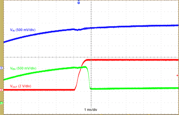
After adding the proposed circuit, the startup waveform is shown in Figure 3-1.
- When the VIN is lower than 1.7 V, the TPS61022 device shuts down. The VOUT is zero and the EN pin voltage is equal to the input voltage.
- After VIN > 1.7 V, the TPS61022 device starts to operate. The VOUT ramps up to 5 V. Then Q1 turns on and the EN pin voltage decreases to 0.6 V. If the VEN is still higher than the EN pin logic low threshold, the device keeps operating.
 Figure 3-1 Startup After Adding Proposed Circuit
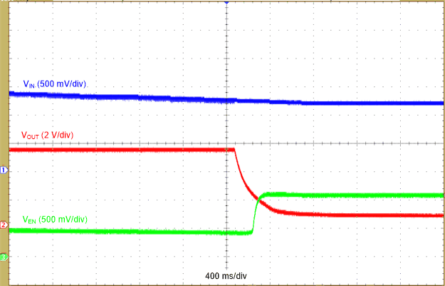
The Figure 3-2 shows the shutdown waveform at 1-mA load condition as the VIN deceases. As the VIN decreases toward 1.2 V, the EN also decreases toward 0.42 V. Once the EN pin voltage is lower than 0.42 V, the device stops operating and VOUT decreases. After VOUT decreases below approximately 2.4 V, Q1 turns off and the VEN becomes equal to VIN again. The VIN is lower than 1.7 V, so the device does not restart, although the EN pin becomes logic high again.
 Figure 3-2 Shutdown at 1-mA Condition
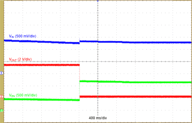
Figure 3-3 shows the shutdown waveform at the 500-mA load condition. The boost converter shuts down when VIN is lower than 1.2 V as designed. Because of the voltage drop across the input cable, the input voltage increases 100 mV after device shuts down.
 Figure 3-3 Shutdown at 500-mA Load