High-Precision Negative-Voltage APD Power Supply Design with TPS61391
Trademarks
All trademarks are the property of their respective owners.
1 Introduction
The TPS61391 is a fully integrated boost converter with an 85-V FET to convert a low input voltage to a higher voltage for biasing the APD. The TPS61391 supports an input voltage ranging from 2.5 V to 5.5 V, the maximum output voltage can reach 85 V. In some applications, for example, mechanically scanning LIDAR, robot LIDAR, or laser distance meters, negative voltage biased APD were also used, the voltage range is from -20 V to -150 V or even lower. Those negative supply voltage need to be of high precision, low ripple, and small solution size.
This application note delivers a low cost, high-precision and small-sized power supply design for the negative-voltage-biased APD application with TPS61391. The output voltage is tightly regulated at a certain value regardless of the line voltage or load current change. This design can cooperate with trans-impedance amplifier, similar to LMH32401 for light detection and ranging (LIDAR) applications, or laser distance measurement systems.
2 Design Process
2.1 Schematic Design
Figure 2-1 shows the schematic of this application note. To achieve -90 V output, two negative charge-pump cells were used. The maximum output voltage of TPS61391 can reach 85 V, so if the required negative voltage is within 0 to -80 V, only one charge pump cell needed; if the required negative voltage is within -80 to -160 V, two charge pump cells should be adopted.
To convert the negative output voltage to a positive feedback voltage, a level shift circuit is implemented. It uses a current mirror circuit built with two inexpensive PNP transistors, and one NPN transistor to regulate the output voltage. For best performance and tighter regulation accuracy, a matched pair can be used, so that the two VBE can be canceled out.
 Figure 2-1 3.3 V Input -90 V Output
Conversion with TPS61391
Figure 2-1 3.3 V Input -90 V Output
Conversion with TPS613912.2 Parameter Calculation
During normal working, the current IFB flowing through R2 and Q2 equals to Vref/R2. The current flowing through Q1 is effected by the VBE mismatch of Q1 and Q2, but the VBE mismatch can be reduced to a minimum level by using matched double transistors in the design. For the PNP matched double transistors, the VBE mismatch is lower than 2mV, neglect this mismatch, IQ1 can be derived from the below equation:

The output voltage equals to:
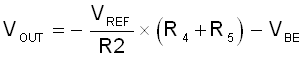
The precision of the output voltage is mainly determined by the tolerance of the output voltage dividing network R2, R4 and R5, the tolerance of the reference voltage Vref and VBE. Set IFB = 50uA, then R2 = 24k ohm based on 1.2 V reference voltage. The value of R1 and R3 is limited by the minimum input voltage, therefore a 20k ohm resistor is chosen in this application note. The total value of R4 and R5 can be calculated by below equation:
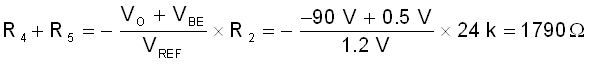
In this application note, the total value of R4 and R5 is set at 1797k ohm, which is quite close to the calculated value.
The output voltage drift caused by the VBE mismatch of the PNP matched double transistors Q1 and Q2 can be calculated by the below equations:


In this application note, BCM857BS is chosen for its <2m V small VBE mismatch.