SLVAF01 October 2020 TPS55340
3.1 Initial Key Designs and Test Results
- VIN_Max: 18VDC, VOUT: 14 V, IOUT: 1.6A
- Set VOR to 10 V from Vout and turn ratio of Np, Ns (Np : Primary turns, Ns: Secondary turns)
- Main check lists from TPS55430 D/S (5A, 40 V Current mode Integrated-FET DC converter)
Table 3-1 Primary Peak Current Should Not Touch IC's
Internal Current Limit Once VOR is Set
|
Parameter |
Test Conditions |
MIN |
TYP |
MAX |
UNIT |
|
|---|---|---|---|---|---|---|
|
OCP and SS |
||||||
|
ILIM |
N-Channel MOSFET current limit |
D = Dmax |
5.25 |
6.6 |
7.775 |
A |
Table 3-2 Absolute Maximum Rating of Vsw should be less than 40
V
|
MIN |
MAX |
UNIT |
||
|---|---|---|---|---|
|
Output voltage |
SW(2) |
-0.3 |
40 |
V |
|
SW (10<10 ns transient)(2) |
-5 |
40 |
V |
|
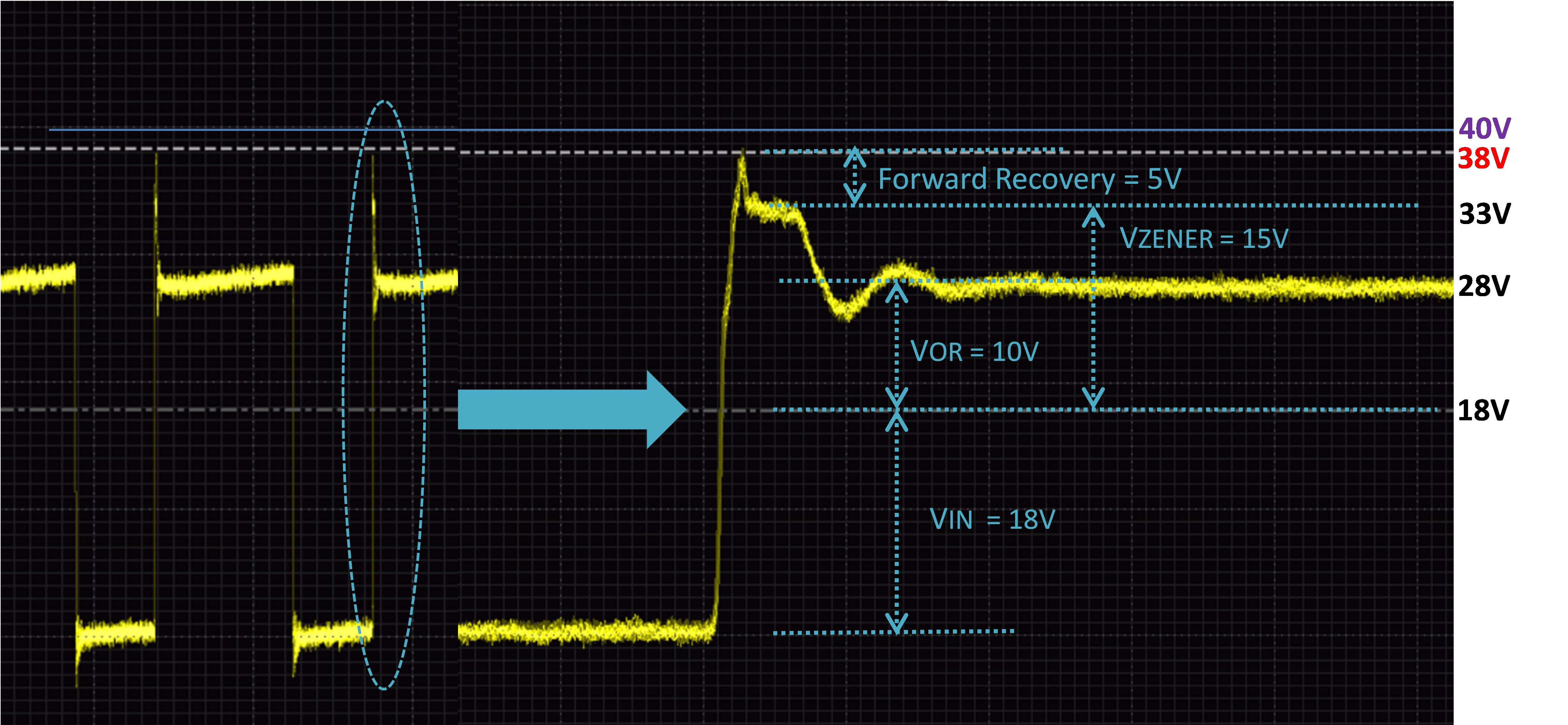
Figure 3-1 is scope image of Vsw on TPS55340 with initial design. Peak Vsw is measured to 38 V. So it has only 2 V margin to its’ AMR rating. Sometimes,in the field, the peak Vsw is required to be less than 80~85% of IC’s AMR to reinforce reliability for mass production. So it needs to be reduced by redesign parameters around TPS55340.
 Figure 3-1 Scope Image on VSW of TPS55430
from Initial Design